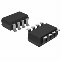
MAX1117EKA+T Maxim Integrated Products, MAX1117EKA+T Datasheet - Page 8

MAX1117EKA+T
Manufacturer Part Number
MAX1117EKA+T
Description
IC ADC 8BIT SERIAL SOT23-8
Manufacturer
Maxim Integrated Products
Datasheet
1.MAX1118EKAT.pdf
(14 pages)
Specifications of MAX1117EKA+T
Number Of Bits
8
Sampling Rate (per Second)
100k
Data Interface
MICROWIRE™, QSPI™, Serial, SPI™
Number Of Converters
1
Power Dissipation (max)
410µW
Voltage Supply Source
Single Supply
Operating Temperature
-40°C ~ 85°C
Mounting Type
Surface Mount
Package / Case
SOT-23-8
Number Of Adc Inputs
2
Architecture
SAR
Conversion Rate
100 KSPs
Resolution
8 bit
Interface Type
3-Wire (SPI, QSPI, MICROWIRE)
Voltage Reference
Internal 2.048 V
Supply Voltage (max)
3.6 V
Supply Voltage (min)
2.7 V
Maximum Power Dissipation
714 mW
Maximum Operating Temperature
+ 85 C
Mounting Style
SMD/SMT
Minimum Operating Temperature
- 40 C
Lead Free Status / RoHS Status
Lead free / RoHS Compliant
Other names
MAX1117EKA+TTR
The MAX1117/MAX1118/MAX1119 ADCs use a suc-
cessive-approximation conversion technique and input
T/H circuitry to convert an analog signal to an 8-bit digi-
tal output. The SPI/QSPI/MICROWIRE compatible inter-
face directly connects to microprocessors (µPs) without
additional circuity (Figure 3).
The input architecture of the ADC is illustrated in Figure
4’s equivalent-input circuit and is composed of the T/H,
the input multiplexer, the input comparator, the
switched capacitor DAC, and the auto-zero rail.
The acquisition interval begins with the falling edge of
CNVST. During the acquisition interval, the analog
Single-Supply, Low-Power,
2-Channel, Serial 8-Bit ADCs
Figure 1. Load Circuits for Enable Time
Figure 3. Typical Operating Circuit
8
ANALOG
DOUT
INPUTS
_______________________________________________________________________________________
1μF
3kΩ
* MAX1118 ONLY
a) V
OL
CH1
GND
CH0
REF*
TO V
MAX1117
MAX1118
MAX1119
OH
CNVST
DOUT
SCLK
GND
V
Detailed Description
DD
C
LOAD
0.1μF
b) HIGH-Z to V
DOUT
1μF
V
DD
V
DD
OL
MISO (SI)
V
I/O
SCK (SK)
DD
3kΩ
AND V
C
GND
LOAD
Track/Hold
CPU
GND
OH
to V
OL
inputs (CH0, CH1) are connected to the holding capac-
itor (C
T/H switch opens and C
retaining the charge on C
nal at the analog input.
Sufficiently low source impedance is required to ensure
an accurate sample. A source impedance <1.5kΩ is
recommended for accurate sample settling. A 100pF
capacitor at the ADC inputs will also improve the accu-
racy of an input sample.
The MAX1117/MAX1118/MAX1119 conversion process
is internally timed. The total acquisition and conversion
process takes <7.5µs. Once an input sample has been
acquired, the comparator’s negative input is then con-
Figure 2. Load Circuits for Disable Time
Figure 4. Equivalent Input Circuit
GND
CH0
CH1
DOUT
HOLD
3kΩ
). Once the acquisition has completed, the
a) V
GND
OH
CAPACITIVE DAC
TO HIGH-Z
HOLD
C
16pF
HOLD
HOLD
HOLD
C
TRACK
R
6.5kΩ
LOAD
IN
as a sample of the sig-
is connected to GND,
Conversion Process
DOUT
b) V
OL
V
TO HIGH-Z
DD
COMPARATOR
3kΩ
AUTOZERO
C
GND
LOAD
RAIL


