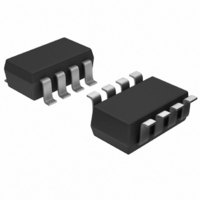
MAX1119EKA+T Maxim Integrated Products, MAX1119EKA+T Datasheet - Page 12

MAX1119EKA+T
Manufacturer Part Number
MAX1119EKA+T
Description
IC ADC 8-BIT 100KSPS SOT23-8
Manufacturer
Maxim Integrated Products
Datasheet
1.MAX1118EKAT.pdf
(14 pages)
Specifications of MAX1119EKA+T
Number Of Bits
8
Sampling Rate (per Second)
100k
Data Interface
MICROWIRE™, QSPI™, Serial, SPI™
Number Of Converters
1
Power Dissipation (max)
180µW
Voltage Supply Source
Single Supply
Operating Temperature
-40°C ~ 85°C
Mounting Type
Surface Mount
Package / Case
SOT-23-8
Number Of Adc Inputs
2
Architecture
SAR
Conversion Rate
100 KSPs
Resolution
8 bit
Interface Type
3-Wire (SPI, QSPI, MICROWIRE)
Voltage Reference
Internal 4.096 V
Supply Voltage (max)
5.5 V
Supply Voltage (min)
4.5 V
Maximum Power Dissipation
714 mW
Maximum Operating Temperature
+ 85 C
Mounting Style
SMD/SMT
Minimum Operating Temperature
- 40 C
Lead Free Status / RoHS Status
Lead free / RoHS Compliant
Other names
MAX1119EKA+TTR
When power is first applied, the MAX1117/MAX1118/
MAX1119 are in AutoShutdown state (<1μA typ). A conver-
sion can be started by toggling CNVST high to low. Powering
up the MAX1117/MAX1118/MAX1119 with CNVST low will
not start a conversion. Conversions initiated prior to the
external reference settling (MAX1118) will result in errors.
Thus, it is necessary to allow the external reference to stabi-
lize prior to initiating a conversion.
The MAX1117/MAX1118/MAX1119 are designed to
automatically shutdown once a conversion is complete
without any external control. An input sample and con-
version process will typically take 5µs to complete, dur-
ing which time the supply current to the analog
sections of the device is fully on. All analog circuitry is
shutdown after a conversion completes, which results
in a supply current of <1µA (see Shutdown Current vs.
Supply Voltage Plot in the Typical Operating
Characteristics). The digital conversion result is main-
tained in a static register and is available for access
through the serial interface at any time.
The power consumption consequence of this architec-
ture is dramatic when relatively slow conversion rates
are needed. For example, at a conversion rate of
10ksps, the average supply current for the MAX1117 is
Single-Supply, Low-Power,
2-Channel, Serial 8-Bit ADCs
Figure 7. Input/Output Transfer Function
12
11111111
11111110
11111101
00000011
00000010
00000001
00000000
______________________________________________________________________________________
OUTPUT CODE
AutoShutDown and Supply Current
0
1
Applications Information
2
INPUT VOLTAGE (LSB)
3
FULL-SCALE
TRANSITION
Power-On Reset
Requirements
FS - 1 1/2 LSB
FS = V
1LSB = V
FS
REF
256
REF
15µA, while at 1ksps it drops to 1.5µA and at 0.1ksps it
is just 0.3µA, or a miniscule 1µW of power consumption
(see Average Supply Current vs. Conversion Rate Plot
in the Typical Operating Characteristics).
Connect an external reference between +1V and V
at the REF pin. The DC input impedance at REF is
extremely high, consisting of leakage current only
(10nA typ). During a conversion, the reference must be
able to deliver up to 20µA average load current and
have an output impedance of 100Ω or less. If the refer-
ence has higher output impedance or is noisy, bypass
it close to the REF pin with a 10nF or larger capacitor.
Figure 7 depicts the input/output transfer function.
Output coding is binary with a +2.048V reference 1LSB
= 8mV (V
For best performance, the board layout should ensure
that digital and analog signal lines are separated from
each other. Do not run analog and digital (especially
clock) lines parallel to one another or run digital lines
underneath the ADC package.
Figure 8 shows the recommended system-ground con-
nections. A single-point analog ground (star-ground
point) should be established at the ADC ground.
Connect all analog grounds to the star ground. The
ground return to the power supply for the star ground
Figure 8. Power-Supply Connections
*OPTIONAL
External Voltage Reference (MAX1118)
GND
GND
REF
/256).
Layout, Grounding, Bypassing
MAX1117
MAX1118
MAX1119
0.1μF
SYSTEM POWER SUPPLIES
1μF
V
DD
Transfer Function
10Ω*
DGND
CIRCUITRY
DIGITAL
+3V/+5V
V
DD
DD


