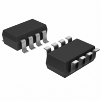
MAX1116EKA+T Maxim Integrated Products, MAX1116EKA+T Datasheet - Page 6

MAX1116EKA+T
Manufacturer Part Number
MAX1116EKA+T
Description
IC ADC 8BIT SERIAL SOT23-8
Manufacturer
Maxim Integrated Products
Datasheet
1.MAX1115EKAT.pdf
(12 pages)
Specifications of MAX1116EKA+T
Number Of Bits
8
Sampling Rate (per Second)
100k
Data Interface
MICROWIRE™, QSPI™, Serial, SPI™
Number Of Converters
1
Power Dissipation (max)
910µW
Voltage Supply Source
Single Supply
Operating Temperature
-40°C ~ 85°C
Mounting Type
Surface Mount
Package / Case
SOT-23-8
Number Of Adc Inputs
1
Architecture
SAR
Conversion Rate
100 KSPs
Resolution
8 bit
Interface Type
Serial
Voltage Reference
Internal 4.096 V
Supply Voltage (max)
5 V
Mounting Style
SMD/SMT
Lead Free Status / RoHS Status
Lead free / RoHS Compliant
Other names
MAX1116EKA+TTR
The MAX1115/MAX1116 ADCs use a successive-
approximation conversion technique and input
track/hold (T/H) circuitry to convert an analog signal to
an 8-bit digital output. The SPI/QSPI/MICROWIRE-
compatible interface directly connects to microproces-
sors (µPs) without additional circuitry (Figure 3).
The input architecture of the ADC is illustrated in the
equivalent-input circuit shown in Figure 4 and is com-
posed of the T/H, input multiplexer, input comparator,
switched capacitor DAC, and auto-zero rail.
The acquisition interval begins with the falling edge of
CNVST. During the acquisition interval, the analog input
(CH0) is connected to the hold capacitor (C
Once the acquisition is complete, the T/H switch opens
and C
charge on C
log input.
Single-Supply, Low-Power, Serial 8-Bit ADCs
Figure 1. Load Circuits for Enable Time
6
DOUT
_______________________________________________________________________________________
PIN
3, 5
HOLD
1
2
4
6
7
8
3kΩ
a) V
OL
HOLD
is connected to GND, which retains the
GND
TO V
OH
CNVST
NAME
DOUT
SCLK
GND
CH0
V
as a sample of the signal at the ana-
I.C.
DD
Detailed Description
C
LOAD
Positive Supply Voltage
Analog Voltage Input
Internally Connected. Connect to ground.
Ground
Convert/Start Input. CNVST initiates a power-up and starts a conversion on its falling edge.
Serial Data Output. Data is clocked out on the falling edge of SCLK. DOUT goes low at the start of a
conversion and presents the MSB at the completion of a conversion. DOUT goes high impedance
once data has been fully clocked out.
Serial Clock. Used for clocking out data on DOUT.
b) HIGH-Z TO V
DOUT
V
DD
OL
Track/Hold
AND V
3kΩ
C
GND
LOAD
OH
TO V
HOLD
OL
).
Sufficiently low source impedance is required to ensure
an accurate sample. A source impedance of <1.5kΩ is
recommended for accurate sample settling. A 100pF
capacitor at the ADC inputs also improves the accuracy
of an input sample.
The MAX1115/MAX1116 conversion process is internal-
ly timed. The total acquisition and conversion process
takes <7.5µs. Once an input sample has been
acquired, the comparator’s negative input is then con-
nected to an auto-zero supply. Since the device
requires only a single supply, the negative input of the
comparator is set to equal V
restores the positive input to V
bit resolution. This action is equivalent to transferring a
charge Q
weighted capacitive DAC, which forms a digital repre-
sentation of the analog-input signal.
Figure 2. Load Circuits for Disable Time
DOUT
FUNCTION
3kΩ
IN
= 16pF
a) V
GND
OH
TO HIGH-Z
✕
V
IN
C
LOAD
from C
DD
Conversion Process
DD
Pin Description
/2. The capacitive DAC
/2 within the limits of 8-
DOUT
HOLD
b) V
OL
V
TO HIGH-Z
to the binary-
DD
3kΩ
C
GND
LOAD


