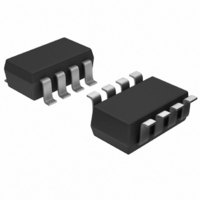
MAX11600EKA+T Maxim Integrated Products, MAX11600EKA+T Datasheet - Page 15

MAX11600EKA+T
Manufacturer Part Number
MAX11600EKA+T
Description
IC ADC SERIAL 8BIT 4CH SOT23-8
Manufacturer
Maxim Integrated Products
Datasheet
1.MAX11602EEE.pdf
(23 pages)
Specifications of MAX11600EKA+T
Number Of Bits
8
Sampling Rate (per Second)
188k
Data Interface
I²C, Serial
Number Of Converters
1
Power Dissipation (max)
1.75mW
Voltage Supply Source
Single Supply
Operating Temperature
-40°C ~ 85°C
Mounting Type
Surface Mount
Package / Case
SOT-23-8
Resolution
8 bit
Interface Type
I2C
Snr
49 dB
Voltage Reference
4.096 V
Supply Voltage (max)
5.5 V
Supply Voltage (min)
4.5 V
Maximum Power Dissipation
567 mW
Maximum Operating Temperature
+ 85 C
Mounting Style
SMD/SMT
Input Voltage
5 V
Minimum Operating Temperature
- 40 C
Lead Free Status / RoHS Status
Lead free / RoHS Compliant
Other names
MAX11600EKA+T
MAX11600EKA+TTR
MAX11600EKA+TTR
The configuration and setup registers (Tables 1 and 2)
default to a single-ended, unipolar, single-channel con-
version on AIN0 using the internal clock with V
reference and AIN_/REF (MAX11600/MAX11601/
MAX11604/MAX11605) configured as an analog input.
For the MAX11602/MAX11603, the REF pin is floating
after power-up. The RAM contents are unknown after
power-up.
SEL[2:0] of the setup byte (Tables 1 and 6) controls the
state of the reference and AIN_/REF (MAX11600/
MAX11601/MAX11604/MAX11605) or REF (MAX11602/
MAX11603). If automatic shutdown is selected (SEL[2:0] =
100), shutdown occurs between conversions when the
MAX11600–MAX11605 are idle. When operating in exter-
nal clock mode, a STOP condition must be issued to place
the devices in idle mode and benefit from automatic shut-
down. A STOP condition is not necessary in internal clock
mode to benefit from automatic shutdown because power-
down occurs once all contents are written to memory
(Figure 10). All analog circuitry is inactive in shutdown and
supply current is less than 1µA. The digital conversion
results are maintained in RAM during shutdown and are
available for access through the serial interface at any
time prior to a STOP or repeated START condition.
When idle, the MAX11600–MAX11605 wait for a START
condition followed by their slave address (see the
Slave Address section). Upon reading a valid address
byte, the MAX11600–MAX11605 power up. The analog
circuits do not require any wakeup time from shutdown,
whether using external or internal reference.
Table 2. Configuration Byte Format
(MSB)
BIT 7
REG
BIT
7
6
5
4
3
2
1
0
2.7V to 3.6V and 4.5V to 5.5V, Low-Power,
Applications Information
4-/8-/12-Channel 2-Wire Serial 8-Bit ADCs
______________________________________________________________________________________
SGL/DIF
SCAN1
SCAN1
SCAN0
NAME
BIT 6
REG
CS3
CS2
CS1
CS0
Register bit. 1 = setup byte (Table 1), 0 = configuration byte.
Scan select bits. Two bits select the scanning configuration (Table 5). Default to 00 at
power-up.
Channel select bits. Four bits select which analog input channels are to be used for conversion
(Tables 3 and 4). Default to 0000 at power-up. For the MAX11600/MAX11601, CS3 and CS2 are
internally set to 0. For the MAX11602/MAX11603, CS3 is internally set to zero.
1 = single-ended, 0 = pseudo-differential (Tables 3 and 4). Default to 1 at power-up (see the
Single-Ended/Pseudo-Differential Input section).
Automatic Shutdown
SCAN0
BIT 5
Power-On Reset
DD
BIT 4
CS3
as the
Automatic shutdown results in dramatic power savings,
particularly at slow conversion rates. For example, at a
conversion rate of 10ksps, the average supply current
for the MAX1036 is 8µA and drops to 2µA at 1ksps.
At 0.1ksps the average supply current is just 1µA (see
Average Supply Current vs. Conversion Rate in the
Typical Operating Characteristics section).
SEL[2:0] of the setup byte (Table 1) controls the refer-
ence and the AIN_/REF (MAX11600/MAX11601/
MAX11604/MAX11605) or REF (MAX11602/MAX11603)
configuration (Table 6). When AIN_/REF (MAX11600/
MAX11601/MAX11604/MAX11605) is configured to be
a reference input or reference output (SEL1 = 1), con-
versions on AIN_/REF appear as if AIN_/REF is con-
nected to GND (see note 2 of Tables 3 and 4).
The internal reference is 4.096V for the MAX11600/
MAX11602/MAX11604 and 2.048V for the MAX11601/
MAX11603/MAX11605. SEL1 of the setup byte controls
whether AIN_/REF (MAX11600/MAX11601/MAX11604/
MAX11605) is used for an analog input or a reference
(Table 6). When AIN_/REF (MAX11600/MAX11601/
MAX11604/MAX11605) or REF (MAX11602/MAX11603) is
configured to be an internal reference output (SEL[2:1] =
11), decouple AIN_/REF (MAX11600/MAX11601/
MAX11604/MAX11605) or REF (MAX11602/MAX11603)
to GND with a 0.01µF capacitor. Due to the decoupling
capacitor and the 675Ω reference source impedance,
allow 80µs for the reference to stabilize during initial
power-up. Once powered up, the reference always
remains on until reconfigured. The reference should not
be used to supply current for external circuitry. When the
MAX11602/MAX11603 is in shutdown, the internal refer-
ence output is in a high-impedance state.
BIT 3
CS2
DESCRIPTION
BIT 2
CS1
BIT 1
Reference Voltage
CS0
Internal Reference
SGL/DIF
(LSB)
BIT 0
15


