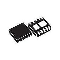
MAX11102ATB+T Maxim Integrated Products, MAX11102ATB+T Datasheet - Page 27

MAX11102ATB+T
Manufacturer Part Number
MAX11102ATB+T
Description
IC ADC 12BIT SPI/SRL 10TDFN
Manufacturer
Maxim Integrated Products
Datasheet
1.MAX11117AUTT.pdf
(30 pages)
Specifications of MAX11102ATB+T
Number Of Bits
12
Sampling Rate (per Second)
2M
Data Interface
MICROWIRE™, QSPI™, Serial, SPI™
Number Of Converters
1
Power Dissipation (max)
1.95W
Voltage Supply Source
Single Supply
Operating Temperature
-40°C ~ 125°C
Mounting Type
Surface Mount
Package / Case
10-WFDFN Exposed Pad
Conversion Rate
2 MSPs
Resolution
12 bit
Interface Type
Serial (3-Wire, SPI, QSPI, Microwire)
Snr
73 dB
Voltage Reference
1 V
Supply Voltage (max)
3.6 V
Supply Voltage (min)
2.2 V
Maximum Power Dissipation
1951 mW
Maximum Operating Temperature
+ 125 C
Mounting Style
SMD/SMT
Input Voltage
2.2 V to 3.6 V
Minimum Operating Temperature
- 40 C
Lead Free Status / RoHS Status
Lead free / RoHS Compliant
Other names
MAX11102ATB+TTR
and stays within a given error band centered on the
resulting steady-state amplifier output level. The
input sampling capacitor charges during the sampling
cycle, referred to as the acquisition period. During this
acquisition period, the settling time is affected by the
input resistance and the input sampling capacitance.
This error can be estimated by looking at the settling of
an RC time constant using the input capacitance and
the source impedance over the acquisition time period.
Figure
MAX4430, offering a settling time of 37ns at 16 bits, is
an excellent choice for this application. See the THD
vs. Input Resistance graph in the Typical Operating
Characteristics.
Figure 17. Typical Application Circuit
17 shows a typical application circuit. The
AIN1
AIN2
V
V
DC
DC
______________________________________________________________________________________
500I
500I
0.1µF
0.1µF
3
4
3
4
MAX4430
MAX4430
+5V
+5V
5
2
5
2
100pF COG
100pF COG
500I
500I
0.1µF
0.1µF
10µF
10µF
1
1
-5V
-5V
10µF
10µF
10I
10I
ADC
0.1µF
COG CAPACITOR
COG CAPACITOR
2Msps/3Msps, Low-Power,
3V
Serial 12-/10-/8-Bit ADCs
470pF
470pF
0.1µF
10µF
10µF
For devices using an external reference, the choice of
the reference determines the output accuracy of the
ADC. An ideal voltage reference provides a perfect initial
accuracy and maintains the reference voltage indepen-
dent of changes in load current, temperature, and time.
Considerations in selecting a reference include initial
voltage accuracy, temperature drift, current source,
sink capability, quiescent current, and noise.
shows a typical application circuit using the MAX6126
to provide the reference voltage. The MAX6033 and
MAX6043 are also
AGND
AIN1
AIN2
V
REF
DD
7
8
4
3
OUTF
OUTS
GNDS
GND
MAX11102
MAX11103
MAX11106
MAX11111
MAX6126
EP
excellent
NR
IN
OVDD
SCLK
DOUT
CS
CHSEL
2
1
V
Choosing a Reference
OVDD
choices.
MISO
1µF
0.1µF
0.1µF
SCK
SS
CPU
+5V
10µF
0.1µF
Figure
27
17


