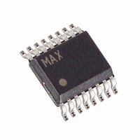
MAX1139EEE+ Maxim Integrated Products, MAX1139EEE+ Datasheet - Page 15

MAX1139EEE+
Manufacturer Part Number
MAX1139EEE+
Description
IC ADC 10-BIT I2C 94.4K 16-QSOP
Manufacturer
Maxim Integrated Products
Datasheet
1.MAX1136EUA.pdf
(22 pages)
Specifications of MAX1139EEE+
Number Of Bits
10
Sampling Rate (per Second)
94.4k
Data Interface
I²C, Serial
Number Of Converters
1
Power Dissipation (max)
2mW
Voltage Supply Source
Single Supply
Operating Temperature
-40°C ~ 85°C
Mounting Type
Surface Mount
Package / Case
16-SSOP (0.150", 3.90mm Width)
Number Of Adc Inputs
12
Architecture
SAR
Conversion Rate
94.4 KSPs
Resolution
10 bit
Interface Type
I2C
Voltage Reference
Internal 2.048 V
Supply Voltage (max)
3.3 V
Mounting Style
SMD/SMT
Lead Free Status / RoHS Status
Lead free / RoHS Compliant
Table 4. Channel Selection in Differential Mode (SGL/DIF = 0)
1. For MAX1136/MAX1137, CS3 and CS2 are internally set to 0.
2. When SEL1 = 1, a differential read between AIN2 and AIN3/REF (MAX1136/MAX1137) or AIN10 and AIN11/REF
A read cycle must be initiated to obtain conversion
results. Read cycles begin with the bus master issuing
a START condition followed by seven address bits and
a read bit (R/W = 1). If the address byte is successfully
received, the MAX1136–MAX1139 (slave) issues an
acknowledge. The master then reads from the slave.
The result is transmitted in two bytes; first six bits of the
first byte are high, then MSB through LSB are consecu-
tively clocked out. After the master has received the
byte(s) it can issue an acknowledge if it wants to con-
tinue reading or a not-acknowledge if it no longer wish-
es to read. If the MAX1136–MAX1139 receive a not-
acknowledge, they release SDA allowing the master to
generate a STOP or a repeated START condition. See
the Clock Mode and Scan Mode sections for detailed
information on how data is obtained and converted.
The clock mode determines the conversion clock and
the data acquisition and conversion time. The clock
mode also affects the scan mode. The state of the set-
up byte’s CLK bit determines the clock mode (Table 1).
CS3
0
0
0
0
0
0
0
0
1
1
1
1
1
1
1
1
(MAX1138/MAX1139) will return the difference between GND and AIN2 or AIN10, respectively. For example, a differential read of
1011 will return the negative difference between AIN10 and GND. In differential scanning, the address increments by 2 until limit set
by CS3:CS1 has been reached.
1
CS2
0
0
0
0
1
1
1
1
0
0
0
0
1
1
1
1
1
2.7V to 3.6V and 4.5V to 5.5V, Low-Power,
CS1
0
0
1
1
0
0
1
1
0
0
1
1
0
0
1
1
______________________________________________________________________________________
4-/12-Channel, 2-Wire Serial 10-Bit ADCs
CS0
0
1
0
1
0
1
0
1
0
1
0
1
0
1
0
1
AIN0
+
-
Data Byte (Read Cycle)
AIN1
+
-
Clock Modes
AIN2
+
-
AIN3
+
-
2
AIN4
+
-
At power-up the MAX1136–MAX1139 are defaulted to
internal clock mode (CLK = 0).
When configured for internal clock mode (CLK = 0), the
MAX1136–MAX1139 use their internal oscillator as the con-
version clock. In internal clock mode, the MAX1136–
MAX1139 begin tracking the analog input after a valid
address on the eighth rising edge of the clock. On the
falling edge of the ninth clock the analog signal is acquired
and the conversion begins. While converting the analog
input signal, the MAX1136–MAX1139 holds SCL low (clock
stretching). After the conversion completes, the results are
stored in internal memory. If the scan mode is set for multi-
ple conversions, they will all happen in succession
with each additional result stored in memory.The
MAX1136/MAX1137 contain four 10-bit blocks of memory,
and the MAX1138/MAX1139 contain twelve 10-bit blocks
of memory. Once all conversions are complete, the
MAX1136–MAX1139 release SCL allowing it to be pulled
high. The master may now clock the results out of the
memory in the same order the scan conversion has been
done at a clock rate of up to 1.7MHz. SCL will be stretched
for a maximum of 7.6µs per channel (see Figure 10).
AIN5
+
RESERVED
RESERVED
RESERVED
RESERVED
-
AIN6
+
-
AIN7
+
-
AIN8
+
-
AIN9
+
-
Internal Clock
AIN10
+
-
AIN11
+
-
15
2


