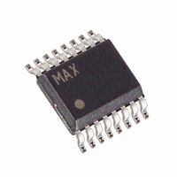
MAX11614EEE+ Maxim Integrated Products, MAX11614EEE+ Datasheet

MAX11614EEE+
Specifications of MAX11614EEE+
Related parts for MAX11614EEE+
MAX11614EEE+ Summary of contents
Page 1
... Power-Down Mode o Software-Configurable Unipolar/Bipolar Applications PART MAX11612EUA+ MAX11613EUA+ MAX11613EWC+* -40°C to +85°C 12 WLP MAX11614EEE+ MAX11615EEE+ MAX11616EEE+ MAX11617EEE+ + Denotes a lead(Pb)-free/RoHs-compliant package. * Future product—contact factory for availability. Pin Configurations, Typical Operating Circuit, and Selector Guide appear at end of data sheet. ...
Page 2
Low-Power, 4-/12-Channel, 2-Wire Serial, 12-Bit ADCs ABSOLUTE MAXIMUM RATINGS V to GND ..............................................................-0.3V to +6V DD AIN0–AIN11, REF to GND ............-0.3V to the lower of (V SDA, SCL to GND.....................................................-0.3V to +6V Maximum ...
Page 3
ADCs in Ultra-Small Packages ELECTRICAL CHARACTERISTICS (continued 2.7V to 3.6V (MAX11613/MAX11615/MAX11617 (MAX11613/MAX11615/MAX11617), V REF otherwise noted. Typical values are at T PARAMETER SYMBOL Throughput Rate f SAMPLE Track/Hold Acquisition Time Internal Clock Frequency Aperture Delay ...
Page 4
Low-Power, 4-/8-/12-Channel, I 12-Bit ADCs in Ultra-Small Packages ELECTRICAL CHARACTERISTICS (continued 2.7V to 3.6V (MAX11613/MAX11615/MAX11617 (MAX11613/MAX11615/MAX11617), V REF otherwise noted. Typical values are at T PARAMETER SYMBOL POWER REQUIREMENTS Supply Voltage Supply Current Power-Supply Rejection Ratio ...
Page 5
ADCs in Ultra-Small Packages TIMING CHARACTERISTICS (Figure 1) (continued 2.7V to 3.6V (MAX11613/MAX11615/MAX11617 (MAX11613/MAX11615/MAX11617), V REF otherwise noted. Typical values are at T PARAMETER SYMBOL TIMING CHARACTERISTICS FOR HIGH-SPEED MODE (C Serial-Clock Frequency f Hold ...
Page 6
Low-Power, 4-/8-/12-Channel, I 12-Bit ADCs in Ultra-Small Packages TIMING CHARACTERISTICS (Figure 1) (continued 2.7V to 3.6V (MAX11613/MAX11615/MAX11617 (MAX11613/MAX11615/MAX11617), V REF otherwise noted. Typical values are at T and for the MAX11612/MAX11614/MAX11616, where N is the number ...
Page 7
ADCs in Ultra-Small Packages (V = 3.3V (MAX11613/MAX11615/MAX11617 94.4ksps, single-ended, unipolar, T SAMPLE AVERAGE SUPPLY CURRENT vs. CONVERSION RATE (EXTERNAL CLOCK) 800 A) INTERNAL REFERENCE ALWAYS ON 750 B) EXTERNAL REFERENCE A 700 650 600 ...
Page 8
Low-Power, 4-/8-/12-Channel, I 12-Bit ADCs in Ultra-Small Packages PIN MAX11612 MAX11614 MAX11613 MAX11615 µMAX WLP A1, A2 — — 8–12 — — — — — — 1 — — — 5 ...
Page 9
ADCs in Ultra-Small Packages SDA SCL V DD GND AIN0 AIN1 AIN2 AIN3 AIN4 AIN5 AIN6 AIN7 AIN8 AIN9 AIN10 AIN11/REF Figure 2. MAX11616/MAX11617 Simplified Functional Diagram SDA I OH Figure 3. Load Circuit Detailed ...
Page 10
Low-Power, 4-/8-/12-Channel, I 12-Bit ADCs in Ultra-Small Packages During the acquisition interval, the T/H switches are in the track position and C charges to the analog input T/H signal. At the end of the acquisition interval, the T/H switches move ...
Page 11
ADCs in Ultra-Small Packages swing from (GND - 0.3V 0.3V) without caus- DD ing damage to the device. For accurate conversions, the inputs must not go more than 50mV below GND or above ...
Page 12
Low-Power, 4-/8-/12-Channel, I 12-Bit ADCs in Ultra-Small Packages A bus master initiates communication with a slave device by issuing a START condition followed by a slave address. When idle, the MAX11612–MAX11617 continu- ously wait for a START condition followed by ...
Page 13
ADCs in Ultra-Small Packages Configuration/Setup Bytes (Write Cycle) A write cycle begins with the bus master issuing a START condition followed by seven address bits (Figure 7) and a write bit (R/W = 0). If the address byte is ...
Page 14
Low-Power, 4-/8-/12-Channel, I 12-Bit ADCs in Ultra-Small Packages Table 2. Configuration Byte Format BIT 7 BIT 6 BIT 5 (MSB) REG SCAN1 SCAN0 BIT NAME 7 REG Register bit setup byte (see Table 1 configuration byte. ...
Page 15
ADCs in Ultra-Small Packages Table 4. Channel Selection in Differential Mode (SGL/DIF = CS3 CS2 CS1 CS0 AIN0 ...
Page 16
Low-Power, 4-/8-/12-Channel, I 12-Bit ADCs in Ultra-Small Packages MASTER TO SLAVE SLAVE TO MASTER A. SINGLE CONVERSION WITH INTERNAL CLOCK CLOCK STRETCH S SLAVE ADDRESS R A RESULT 4 MSBs t ACQ t CONV B. ...
Page 17
ADCs in Ultra-Small Packages Table 5. Scanning Configuration SCAN1 SCAN0 Scans up from AIN0 to the input selected by CS3–CS0. When CS3–CS0 exceeds 1011, the scanning 0 0 stops at AIN11. When AIN_/REF is set REF ...
Page 18
Low-Power, 4-/8-/12-Channel, I 12-Bit ADCs in Ultra-Small Packages Table 6. Reference Voltage, AIN_/REF, and REF Format SEL2 SEL1 SEL0 Don’t ...
Page 19
OUTPUT CODE REF 011 . . . 111 2 011 . . . 110 REF - 000 . . . 010 V REF 000 . . . 001 1 LSB = ...
Page 20
Low-Power, 4-/8-/12-Channel, I 12-Bit ADCs in Ultra-Small Packages Signal-to-Noise Ratio For a waveform perfectly reconstructed from digital sam- ples, the theoretical maximum SNR is the ratio of the full- scale analog input (RMS value) to the RMS quantization error (residual ...
Page 21
ADCs in Ultra-Small Packages Pin Configurations TOP VIEW + AIN0 1 AIN1 2 MAX11612 MAX11613 AIN2 3 6 AIN3/REF 4 μMAX + (REF) AIN11/REF 1 16 (N.C.) AIN10 2 15 (N.C.) AIN9 3 14 MAX11614– (N.C.) AIN8 4 13 ...
Page 22
... Maxim cannot assume responsibility for use of any circuitry other than circuitry entirely embodied in a Maxim product. No circuit patent licenses are implied. Maxim reserves the right to change the circuitry and specifications without notice at any time. 22 _____________________Maxim Integrated Products, 120 San Gabriel Drive, Sunnyvale, CA 94086 408-737-7600 © 2011 Maxim Integrated Products ...


