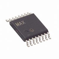
MAX1154BEUE+ Maxim Integrated Products, MAX1154BEUE+ Datasheet - Page 9

MAX1154BEUE+
Manufacturer Part Number
MAX1154BEUE+
Description
IC ADC 10BIT SYS MON 16TSSOP
Manufacturer
Maxim Integrated Products
Datasheet
1.MAX1153BEUE.pdf
(30 pages)
Specifications of MAX1154BEUE+
Number Of Bits
10
Sampling Rate (per Second)
94k
Data Interface
MICROWIRE™, QSPI™, Serial, SPI™
Number Of Converters
1
Power Dissipation (max)
15mW
Voltage Supply Source
Single Supply
Operating Temperature
-40°C ~ 85°C
Mounting Type
Surface Mount
Package / Case
16-TSSOP
Number Of Adc Inputs
10
Architecture
SAR
Conversion Rate
94 KSPs
Resolution
10 bit
Interface Type
Serial
Voltage Reference
Internal 4.096 V or External
Supply Voltage (max)
5 V
Mounting Style
SMD/SMT
Lead Free Status / RoHS Status
Lead free / RoHS Compliant
with Internal Temperature Sensor and V
PIN
10
11
12
13
14
15
16
1
2
3
4
5
6
7
8
9
Stand-Alone, 10-Channel, 10-Bit System Monitors
NAME
DOUT
SCLK
AIN0
AIN1
AIN2
AIN3
AIN4
AIN5
AIN6
AIN7
GND
AIN1
AIN2
AIN3
AIN4
AIN5
AIN6
AIN7
REF
V
DIN
INT
DD
INTERNAL TEMP
CONFIGURATION
ACCUMULATOR
THRESHOLD
THRESHOLD
Serial Data Input. DIN data is latched into the serial interface on the rising edge of the SCLK.
CHANNEL
Analog Voltage Input/Temperature Input Channel 0 or Positive Differential Input Relative to AIN1
Analog Voltage Input/Temperature Input Channel 1 or Negative Differential Input Relative to AIN0
Analog Voltage Input/Temperature Input Channel 2 or Positive Differential Input Relative to AIN3
Analog Voltage Input/Temperature Input Channel 3 or Negative Differential Input Relative to AIN2
Analog Voltage Input/Temperature Input Channel 4 or Positive Differential Input Relative to AIN5
Analog Voltage Input/Temperature Input Channel 5 or Negative Differential Input Relative to AIN4
Analog Voltage Input/Temperature Input Channel 6 or Positive Differential Input Relative to AIN7
Analog Voltage Input/Temperature Input Channel 7 or Negative Differential Input Relative to AIN6
Positive Reference Input in External Mode. Bypass REF with a 0.1μF capacitor to GND when in external mode.
When using the internal reference, REF must be left open.
Interrupt Output. Push-pull or open drain with selectable polarity. See Table 9 and the INT Interrupt Output section.
Serial Data Output. DOUT transitions on the falling edge of SCLK. High impedance when
Ground
Positive Power Supply. Bypass V
Serial Clock Input. SCLK clocks data in and out of the serial interface (duty cycle must be 40% to 60%).
Active-Low Chip-Select Input. When
impedance, and the serial interface resets.
LOWER
UPPER
V
DD
_______________________________________________________________________________________
CONFIGURATION
ACCUMULATOR
THRESHOLD
THRESHOLD
REFERENCE
CHANNEL
SENSOR
LOWER
V
UPPER
TEMP
MUX
DD
/2
CONFIGURATION
ACCUMULATOR
THRESHOLD
THRESHOLD
CHANNEL
LOWER
UPPER
AIN0
CONVERSION
ADC WITH
CONTROL
12-BIT
SCAN
AND
T/H
POR
CONFIGURATION
ACCUMULATOR
THRESHOLD
THRESHOLD
CHANNEL
LOWER
UPPER
AIN1
DD
POWER
GOOD
with a 0.1μF capacitor to GND.
CONFIGURATION
ACCUMULATOR
THRESHOLD
THRESHOLD
is low, the serial interface is enabled. When
CHANNEL
UPPER
LOWER
AIN2
CONFIGURATION
ACCUMULATOR
THRESHOLD
THRESHOLD
CHANNEL
LOWER
FUNCTION
UPPER
AIN3
INPUT CONFIGURATION REGISTER
INPUT CHANNEL REGISTER
STEP-UP REGISTER
ALARM REGISTER
CONFIGURATION
ACCUMULATOR
THRESHOLD
THRESHOLD
CHANNEL
AVERAGING
LOWER
UPPER
AIN4
CONFIGURATION
ACCUMULATOR
THRESHOLD
THRESHOLD
CHANNEL
LOWER
UPPER
AIN5
CONFIGURATION
ACCUMULATOR
THRESHOLD
THRESHOLD
CHANNEL
LOWER
UPPER
AIN6
MAX1153
MAX1154
DD
COMPARATOR
Pin Description
INTERFACE
is high, DOUT is high
Block Diagram
DIGITAL
CONFIGURATION
SERIAL
ACCUMULATOR
THRESHOLD
THRESHOLD
CHANNEL
UPPER
LOWER
AIN7
is at logic high.
Monitor
REF
DOUT
DIN
SCLK
CS
INT
9


