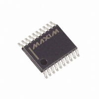
MAX1081BEUP+ Maxim Integrated Products, MAX1081BEUP+ Datasheet - Page 3

MAX1081BEUP+
Manufacturer Part Number
MAX1081BEUP+
Description
IC ADC 10BIT 300KSPS 20-TSSOP
Manufacturer
Maxim Integrated Products
Datasheet
1.MAX1080BEUP.pdf
(24 pages)
Specifications of MAX1081BEUP+
Number Of Bits
10
Sampling Rate (per Second)
300k
Data Interface
MICROWIRE™, QSPI™, Serial, SPI™
Number Of Converters
1
Power Dissipation (max)
8.0mW
Voltage Supply Source
Analog and Digital
Operating Temperature
-40°C ~ 85°C
Mounting Type
Surface Mount
Package / Case
20-TSSOP
Number Of Adc Inputs
8
Architecture
SAR
Conversion Rate
300 KSPs
Resolution
10 bit
Input Type
Differential
Interface Type
4-Wire (SPI, QSPI, MICROWIRE, TMS320)
Voltage Reference
Internal 2.5 V or External
Supply Voltage (max)
3.6 V
Supply Voltage (min)
2.7 V
Maximum Power Dissipation
559 mW
Maximum Operating Temperature
+ 85 C
Mounting Style
SMD/SMT
Minimum Operating Temperature
- 40 C
Lead Free Status / RoHS Status
Lead free / RoHS Compliant
8-Channel, Serial 10-Bit ADCs with Internal Reference
ELECTRICAL CHARACTERISTICS—MAX1080 (continued)
(V
+2.5V at REF, REFADJ = V
ANALOG INPUTS (CH7–CH0, COM)
INTERNAL REFERENCE
EXTERNAL REFERENCE (reference buffer disabled, reference applied to REF)
DIGITAL INPUTS (DIN, SCLK, CS, SHDN)
DIGITAL OUTPUTS (DOUT, SSTRB)
Input Voltage Range, Single
Ended and Differential (Note 6)
Multiplexer Leakage Current
Input Capacitance
REF Output Voltage
REF Short-Circuit Current
REF Output Temperature
Coefficient
Load Regulation (Note 7)
Capacitive Bypass at REF
Capacitive Bypass at REFADJ
REFADJ Output Voltage
REFADJ Input Range
REFADJ Buffer Disable
Threshold
Buffer Voltage Gain
REF Input Voltage Range
REF Input Current
Input High Voltage
Input Low Voltage
Input Hysteresis
Input Leakage
Input Capacitance
Output Voltage Low
Output Voltage High
Three-State Leakage Current
Three-State Output Capacitance
DD1
= V
PARAMETER
DD2
= +4.5V to +5.5V, COM = GND, f
300ksps/400ksps, Single-Supply, Low-Power,
_______________________________________________________________________________________
DD1
, T
A
= T
SYMBOL
TC V
V
C
V
V
V
V
V
V
HYST
C
MIN
CH_
I
REF
OUT
INH
INL
OH
I
IN
OL
IN
L
REF
to T
MAX
Unipolar, V
Bipolar, V
to COM or CH_
On/off leakage current, V
T
0 to 1mA output load
For small adjustments, from 1.22V
To power down the internal reference
(Note 8)
V
V
In power-down mode, f
V
I
I
CS = 5V
CS = 5V
SINK
SOURCE
A
REF
REF
IN
SCLK
, unless otherwise noted. Typical values are at T
= +25°C
= 0 or V
= 2.500V, f
= 2.500V, f
= 5mA
= 6.4MHz, 50% duty cycle, 16 clocks/conversion cycle (400ksps), external
= 1mA
COM
COM
DD2
or V
CONDITIONS
= 0
SCLK
SCLK
CH_
= 6.4MHz
= 0
= V
SCLK
CH_
REF
= 0
= 0 or V
/2, referenced
DD1
2.480
0.01
MIN
4.7
1.4
1.0
3.0
A
4
= +25°C.)
±0.001
+2.05
2.500
±100
TYP
1.22
±15
200
18
0.1
0.2
30
15
15
V
±V
DD1
V
2.520
50mV
V
DD1
±10
350
320
2.0
0.8
0.4
±1
±1
REF
10
10
REF
MAX
5
- 1.0
/2
+
ppm/°C
mV/mA
UNITS
mA
mV
V/V
mA
µA
pF
µF
µF
µA
µA
pF
µA
pF
V
V
V
V
V
V
V
V
V
V
3


