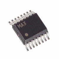
MAX1167BEEE+ Maxim Integrated Products, MAX1167BEEE+ Datasheet - Page 10

MAX1167BEEE+
Manufacturer Part Number
MAX1167BEEE+
Description
IC ADC 16BIT 200KSPS 16-QSOP
Manufacturer
Maxim Integrated Products
Datasheet
1.MAX1167BEEE.pdf
(30 pages)
Specifications of MAX1167BEEE+
Number Of Bits
16
Sampling Rate (per Second)
200k
Data Interface
MICROWIRE™, QSPI™, Serial, SPI™
Number Of Converters
1
Power Dissipation (max)
667mW
Voltage Supply Source
Analog and Digital
Operating Temperature
-40°C ~ 85°C
Mounting Type
Surface Mount
Package / Case
16-SSOP (0.150", 3.90mm Width)
Lead Free Status / RoHS Status
Lead free / RoHS Compliant
Multichannel, 16-Bit, 200ksps Analog-to-Digital
Converters
10
MAX1167
______________________________________________________________________________________
10
11
12
13
14
15
16
—
—
—
—
1
2
3
4
5
6
7
8
9
PIN
MAX1168
10
15
16
17
18
19
20
21
22
11
12
3
4
5
6
7
8
9
1
2
REFCAP
NAME
DGND
AGND
AGND
DOUT
SCLK
AV
DV
DSPR
DSEL
EOC
AIN0
AIN1
AIN2
AIN3
AIN4
AIN5
REF
DIN
CS
DD
DD
Serial Data Output. Data changes state on SCLK’s falling edge in SPI/QSPI/MICROWIRE
mode and on SCLK’s rising edge in DSP mode (MAX1168 only). DOUT is high impedance
when CS is high.
Serial Clock Input. SCLK drives the conversion process in external clock mode and clocks
data out.
Serial Data Input. Use DIN to communicate with the command/configuration/control
register. In SPI/QSPI/MICROWIRE mode, the rising edge of SCLK clocks in data at DIN. In
DSP mode, the falling edge of SCLK clocks in data at DIN.
End-of-Conversion Output. In internal clock mode, a logic low at EOC signals the end of a
conversion with the result available at DOUT. In external clock mode, EOC remains high.
Analog Input 0
Analog Input 1
Analog Input 2
Analog Input 3
Reference Voltage Input/Output. V
with a 10µF capacitor. Bypass with a 1µF (min) capacitor when using internal reference.
Refer ence Byp ass C ap aci tor C onnecti on. Byp ass to AG N D w i th a 0.1µF cap aci tor w hen
usi ng i nter nal r efer ence. Inter nal r efer ence and b uffer shut d ow n i n exter nal r efer ence m od e.
Analog Ground. Connect to pin 18 (MAX1168) or pin 12 (MAX1167).
Primary Analog Ground (Star Ground). Power return for AV
Analog Supply Voltage. Bypass to AGND with a 0.1µF capacitor.
Active-Low Chip-Select Input. Forcing CS high places the MAX1167/MAX1168 in shutdown
with a typical supply current of 0.6µA. In SPI/QSPI/MICROWIRE mode, a high-to-low
transition on CS activates normal operating mode. In DSP mode, after the initial CS
transition from high to low, CS can remain low for the entire conversion process (see the
Operating Modes section).
Digital Ground
Digital Supply Voltage. Bypass to DGND with a 0.1µF capacitor.
DSP Frame-Sync Receive Input. A frame-sync pulse received at DSPR initiates a
conversion. Connect to logic high when using SPI/QSPI/MICROWIRE mode.
Data-Bit Transfer-Select Input. Logic low on DSEL places the device in 8-bit-wide data-
transfer mode. Logic high places the device in 16-bit-wide data-transfer mode. Do not
leave DSEL unconnected.
Analog Input 4
Analog Input 5
REF
sets the analog voltage range. Bypass to AGND
FUNCTION
DD
.
Pin Description


