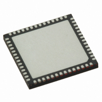
MAX11046ETN+ Maxim Integrated Products, MAX11046ETN+ Datasheet - Page 14

MAX11046ETN+
Manufacturer Part Number
MAX11046ETN+
Description
ADC 16BIT SAMPLING 8CH 56-TQFN
Manufacturer
Maxim Integrated Products
Datasheet
1.MAX11044ETN.pdf
(27 pages)
Specifications of MAX11046ETN+
Number Of Bits
16
Sampling Rate (per Second)
250k
Data Interface
Parallel
Number Of Converters
8
Power Dissipation (max)
2.22W
Voltage Supply Source
Analog and Digital
Operating Temperature
-40°C ~ 85°C
Mounting Type
Surface Mount
Package / Case
56-WQFN Exposed Pad, 56-HWQFN
Number Of Adc Inputs
8
Architecture
SAR
Conversion Rate
250 KSPs
Resolution
16 bit
Input Type
Voltage
Interface Type
Parallel
Snr
92.3 dB
Voltage Reference
Internal 4.096 V
Supply Voltage (max)
5.25 V
Supply Voltage (min)
2.7 V, 4.75 V
Maximum Power Dissipation
2222 mW
Maximum Operating Temperature
+ 85 C
Mounting Style
SMD/SMT
Input Voltage
5 V
Minimum Operating Temperature
- 40 C
Lead Free Status / RoHS Status
Lead free / RoHS Compliant
4-/6-/8-Channel, 16-/14-Bit,
Simultaneous-Sampling ADCs
14
22, 28, 35, 43,
23, 28, 32, 38,
24, 29, 35, 46,
25, 30, 36, 45,
43, 49, 53, 58
MAX11054
(TQFP-EP)
8, 22, 59
9, 21, 60
______________________________________________________________________________________
52, 57
51, 56
26, 55
10
11
12
13
14
15
16
17
18
19
49
1
2
3
4
5
6
7
22, 28, 35, 43,
23, 28, 32, 38,
24, 29, 35, 46,
25, 30, 36, 45,
43, 49, 53, 58
MAX11055
(TQFP-EP)
8, 22, 59
9, 21, 60
52, 57
51, 56
26, 55
PIN
10
11
12
13
14
15
16
17
18
19
49
1
2
3
4
5
6
7
22, 28, 35, 43,
23, 28, 32, 38,
24, 29, 35, 46,
25, 30, 36, 45,
43, 49, 53, 58
MAX11056
(TQFP-EP)
8, 22, 59
9, 21, 60
52, 57
51, 56
26, 55
10
11
12
13
14
15
16
17
18
19
49
1
2
3
4
5
6
7
RDC_SENSE
DB1/CR3
DB0/CR2
CONVST
AGNDS
NAME
DGND
AGND
DVDD
SHDN
AVDD
DB12
DB11
DB10
EOC
DB9
DB8
DB7
DB6
DB5
DB4
DB3
DB2
CR1
CR0
14-Bit Parallel Data Bus Digital Output Bit 5
14-Bit Parallel Data Bus Digital Output Bit 4
14-Bit Parallel Data Bus Digital Output Bit 3
14-Bit Parallel Data Bus Digital Output Bit 2
Configuration Register Input Bit 1
Configuration Register Input Bit 0
conversion is initiated.
sam p l e and star ts a conver si on on the cap tur ed sam p l e.
The AD C i s i n acq ui si ti on m od e w hen C ON V S T i s l ow
and C ON V S T m od e = 0.
Refer ence Buffer S ense Feed b ack. C onnect to RD C p l ane.
14-Bit Parallel Data Bus Digital Output Bit 12
14-Bit Parallel Data Bus Digital Output Bit 11
14-Bit Parallel Data Bus Digital Output Bit 10
14-Bit Parallel Data Bus Digital Output Bit 9
14-Bit Parallel Data Bus Digital Output Bit 8
14-Bit Parallel Data Bus Digital Output Bit 7
14-Bit Parallel Data Bus Digital Output Bit 6
Digital Ground
Digital Supply. Bypass to DGND with a 0.1µF capacitor
at each DVDD input.
14-Bit Parallel Data Bus Digital Output Bit 1/
Configuration Register Input Bit 3
14-Bit Parallel Data Bus Digital Output Bit 0/
Configuration Register Input Bit 2
Active-Low End-of-Conversion Output. EOC goes low
when conversion is completed. EOC goes high when a
C onver t S tar t Inp ut. Ri si ng ed g e of C ON V S T end s
Shutdown Input. If SHDN is held high, the entire device
will enter and stay in a low-current state. Contents of
the configuration register are not lost when in the
shutdown mode.
Signal Ground. Connect all AGND and AGNDS inputs
together on PCB.
Analog Supply Input. Bypass AVDD to AGND with a
0.1µF capacitor at each AVDD input.
Analog Ground. Connect all AGND inputs together.
Pin Description (continued)
FUNCTION


