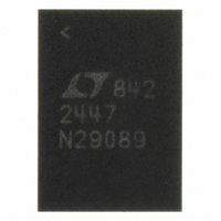
LTC2447IUHF#PBF Linear Technology, LTC2447IUHF#PBF Datasheet - Page 14

LTC2447IUHF#PBF
Manufacturer Part Number
LTC2447IUHF#PBF
Description
IC ADC 24BIT 8CH HI SPEED 38QFN
Manufacturer
Linear Technology
Datasheet
1.LTC2446IUHFPBF.pdf
(28 pages)
Specifications of LTC2447IUHF#PBF
Number Of Bits
24
Sampling Rate (per Second)
8k
Data Interface
MICROWIRE™, Serial, SPI™
Number Of Converters
1
Power Dissipation (max)
40mW
Voltage Supply Source
Single Supply
Operating Temperature
-40°C ~ 85°C
Mounting Type
Surface Mount
Package / Case
38-WFQFN, Exposed Pad
Lead Free Status / RoHS Status
Lead free / RoHS Compliant
Available stocks
Company
Part Number
Manufacturer
Quantity
Price
LTC2446/LTC2447
APPLICATIO S I FOR ATIO
Speed Multiplier Mode
In addition to selecting the speed/resolution, a speed
multiplier mode is used to double the output rate while
maintaining the selected resolution. The last bit of the 5-bit
speed/resolution control word (TWOX, see Table 4) deter-
mines if the output rate is 1x (no speed increase) or 2x
(double the selected speed).
While operating in the 1x mode, the device combines two
internal conversions for each conversion result in order to
remove the ADC offset. Every conversion cycle, the offset
and offset drift are transparently calibrated greatly simpli-
fying the user interface. The conversion result has no
latency. The first conversion following a newly selected
speed/resolution and/or input/reference is valid. This is
identical to the operation of the LTC2440, LTC2444,
LTC2445, LTC2448, LTC2449, LTC2414 and LTC2418.
While operating in the 2x mode, the device performs a
running average of the last two conversion results. This
automatically removes the offset and drift of the device
while increasing the output rate by 2x. The resolution
(noise) remains the same as the 1x mode. If a new
channel/reference is selected, the conversion result is
valid for all conversions after the first conversion (one
cycle latency). If a new speed/resolution is selected, the
first conversion result is valid but the resolution (noise) is
a function of the running average. All subsequent conver-
sion results are valid. If the mode is changed from either
1x to 2x or 2x to 1x without changing the resolution or
channel, the first conversion result is valid.
If an external buffer/amplifier circuit is used for the
LTC2447, the 2x mode can be used to increase the settling
time of the amplifier between readings. While operating in
the 2x mode, the multiplexer output (input to the external
buffer/amplifier) is switched at the end of each conversion
cycle. Prior to concluding the data out/in cycle, the analog
multiplexer output is switched. This occurs at the end of
Table 5. LTC2446/LTC2447 Interface Timing Modes
CONFIGURATION
External SCK, Single Cycle Conversion
External SCK, 3-Wire I/O
Internal SCK, Single Cycle Conversion
Internal SCK, 3-Wire I/O, Continuous Conversion
14
U
U
W
SOURCE
U
External
External
Internal
Internal
SCK
the conversion cycle (just prior to the data output cycle)
for auto calibration. The time required to read the conver-
sion enables more settling time for the external buffer/
amplifier. The offset/offset drift of the external amplifiers
are automatically removed by the converter’s auto calibra-
tion sequence for both the 1x and 2x speed modes.
While operating in the 1x mode, if a new input channel/
reference is selected the multiplexer is switched on the
falling edge of the 14th SCK (once the complete data input
word is programmed). The remaining data output se-
quence time can be used to allow the external buffer/
amplifier to settle.
BUSY
The BUSY output (Pin 2) is used to monitor the state of
conversion, data output and sleep cycle. While the part is
converting, the BUSY pin is HIGH. Once the conversion is
complete, BUSY goes LOW indicating the conversion is
complete and data out is ready. The part now enters the
LOW power sleep state. BUSY remains LOW while data is
shifted out of the device and SDI is shifted into the device.
It goes HIGH at the conclusion of the data input/output
cycle indicating a new conversion has begun. This rising
edge may be used to flag the completion of the data read
cycle.
SERIAL INTERFACE TIMING MODES
The LTC2446/LTC2447’s 3- or 4-wire interface is SPI and
MICROWIRE compatible. This interface offers several flex-
ible modes of operation. These include internal/external
serial clock, 3- or 4-wire I/O, single cycle conversion and
autostart. The following sections describe each of these
serial interface timing modes in detail. In all these cases,
the converter can use the internal oscillator (F
an external oscillator connected to the F
Table 5 for a summary.
CONVERSION
CS and SCK
Continuous
CONTROL
CYCLE
CS ↓
SCK
CS and SCK
CONTROL
OUTPUT
Internal
DATA
CS ↓
SCK
O
CONNECTION
WAVEFORMS
Figures 4, 5
Figures 7, 8
pin. Refer to
Figure 6
Figure 9
O
AND
= LOW) or
24467fa


