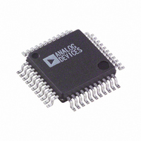
AD7859LASZ Analog Devices Inc, AD7859LASZ Datasheet - Page 22

AD7859LASZ
Manufacturer Part Number
AD7859LASZ
Description
IC ADC 12BIT 8CH 200KSPS 44-MQFP
Manufacturer
Analog Devices Inc
Datasheet
1.AD7859LASZ.pdf
(28 pages)
Specifications of AD7859LASZ
Data Interface
Parallel
Number Of Bits
12
Sampling Rate (per Second)
100k
Number Of Converters
2
Power Dissipation (max)
30mW
Voltage Supply Source
Analog and Digital
Operating Temperature
-40°C ~ 85°C
Mounting Type
Surface Mount
Package / Case
44-MQFP, 44-PQFP
Resolution (bits)
12bit
Sampling Rate
100kSPS
Input Channel Type
Single Ended
Supply Current
1.95mA
Digital Ic Case Style
QFP
No. Of Pins
44
Lead Free Status / RoHS Status
Lead free / RoHS Compliant
Available stocks
Company
Part Number
Manufacturer
Quantity
Price
Company:
Part Number:
AD7859LASZ
Manufacturer:
Analog Devices Inc
Quantity:
10 000
Part Number:
AD7859LASZ
Manufacturer:
ADI/亚德诺
Quantity:
20 000
Company:
Part Number:
AD7859LASZ-REEL
Manufacturer:
Analog Devices Inc
Quantity:
10 000
AD7859/AD7859L
Self-Calibration Timing
Figure 29 shows the timing for a software full self-calibration.
Here the BUSY line stays high for the full length of the self-
calibration. A self-calibration is initiated by writing to the
control register and setting the STCAL bit to 1. The BUSY line
goes high at the end of the write to the control register, and
BUSY goes low when the full self-calibration is complete after a
time t
For the self-(gain + offset), self-offset and self-gain calibrations,
the BUSY line is triggered high at the end of the write to the
control register and stays high for the full duration of the self-
calibration. The length of time for which BUSY is high depends
on the type of self-calibration that is initiated. Typical values are
given in Table IX. The timing diagram for the other self-calibration
options is similar to that outlined in Figure 29.
System Calibration Description
System calibration allows the user to remove system errors ex-
ternal to the AD7859/AD7859L, as well as remove the errors of
the AD7859/AD7859L itself. The maximum calibration range
for the system offset errors is 5% of V
gain errors, it is 2.5% of V
gain errors are outside these ranges, the system calibration algo-
rithm reduces the errors as much as the trim range allows.
Figures 30 through 32 illustrate why a specific type of system
calibration might be used. Figure 30 shows a system offset cali-
bration (assuming a positive offset) where the analog input
range has been shifted upwards by the system offset after the
system offset calibration is completed. A negative offset may
also be removed by a system offset calibration.
SYS OFFSET
V
BUSY
DATA
REF
WR
Figure 29. Timing Diagram for Full Self-Calibration
CS
– 1LSB
MAX SYSTEM OFFSET
CAL
AGND
IS 5% OF V
as show in Figure 29.
Figure 30. System Offset Calibration
HI-Z
REF
ANALOG
INPUT
RANGE
REF
SYSTEM OFFSET
CALIBRATION
VALID
DATA
. If the system offset or system
V
REF
t
19
+ SYS OFFSET
V
SYS OFFSET
MAX SYSTEM FULL SCALE
REF
REF
HI-Z
IS 2.5% FROM V
– 1LSB
DATA LATCHED INTO
CONTROL REGISTER
AGND
MAX SYSTEM OFFSET
and for the system
IS 5% OF V
t
CAL
REF
REF
ANALOG
INPUT
RANGE
–22–
Figure 31 shows a system gain calibration (assuming a system
full scale greater than the reference voltage) where the analog
input range has been increased after the system gain calibration
is completed. A system full-scale voltage less than the reference
voltage may also be accounted for a by a system gain calibration.
Finally in Figure 32 both the system offset error and gain error
are removed by the system offset followed by a system gain cali-
bration. First the analog input range is shifted upwards by the
positive system offset and then the analog input range is adjusted at
the top end to account for the system full scale.
V
SYS OFFSET
SYS FULL S.
V
MAX SYSTEM FULL SCALE
REF
REF
MAX SYSTEM FULL SCALE
IS 2.5% FROM V
SYS F.S.
IS 2.5% FROM V
– 1LSB
– 1LSB
AGND
MAX SYSTEM OFFSET
AGND
Figure 32. System (Gain + Offset) Calibration
IS 5% OF V
Figure 31. System Gain Calibration
ANALOG
INPUT
RANGE
REF
REF
REF
ANALOG
INPUT
RANGE
SYSTEM OFFSET
FOLLOWED BY
CALIBRATION
SYSTEM GAIN
CALIBRATION
SYSTEM GAIN
CALIBRATION
V
REF
+ SYS OFFSET
SYS OFFSET
V
MAX SYSTEM FULL SCALE
V
SYS FULL S.
MAX SYSTEM FULL SCALE
REF
REF
IS 2.5% FROM V
SYS F.S.
IS 2.5% FROM V
– 1LSB
AGND
MAX SYSTEM OFFSET
– 1LSB
AGND
IS 5% OF V
REF
REF
REF
ANALOG
INPUT
RANGE
REV. A
ANALOG
INPUT
RANGE


