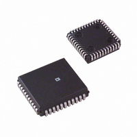
AD7885AAPZ Analog Devices Inc, AD7885AAPZ Datasheet - Page 12

AD7885AAPZ
Manufacturer Part Number
AD7885AAPZ
Description
IC ADC 16BIT SAMPLING HS 44-PLCC
Manufacturer
Analog Devices Inc
Datasheet
1.AD7885AAPZ.pdf
(16 pages)
Specifications of AD7885AAPZ
Number Of Bits
16
Sampling Rate (per Second)
166k
Data Interface
Parallel
Number Of Converters
2
Power Dissipation (max)
325mW
Voltage Supply Source
Dual ±
Operating Temperature
-40°C ~ 85°C
Mounting Type
Surface Mount
Package / Case
44-PLCC
Lead Free Status / RoHS Status
Lead free / RoHS Compliant
AD7884/AD7885
Dynamic Performance
With a combined conversion and acquisition time of 6 µs, the
AD7884/AD7885 is ideal for wide bandwidth signal processing appli-
cations. Signal-to-(noise + distortion), total harmonic distortion,
peak harmonic or spurious noise, and intermodulation distortion
are all specified. Figure 16 shows a typical FFT plot of a 1.8 kHz,
±5 V input after being digitized by the AD7884/AD7885.
Effective Number of Bits
The formula for SNR (see Terminology section) is related to
the resolution or number of bits in the converter. Rewriting the
formula, below, gives a measure of performance expressed in
effective number of bits (N).
The effective number of bits for a device can be calculated from
its measured SNR. Figure 17 shows a typical plot of effective
number of bits versus frequency for the AD7884. The sampling
frequency is 166 kHz.
Figure 17. Effective Number of Bits vs. Frequency
–120
–150
–30
–60
–90
16
15
14
13
12
11
10
0
0
Figure 16. AD7884/AD7885 FFT Plot
f
f
SNR = 87dB
THD = –95dB
IN
SAMPLE
= 1.8kHz,
N
20
= 163kHz
=
(
SNR
5V SINE WAVE
FREQUENCY – kHz
2048 POINT FFT
−
1 76 6 02
40
.
)
.
60
80
–12–
MICROPROCESSOR INTERFACING
The AD7884/AD7885 is designed on a high speed process
that results in very fast interfacing timing (data access time of
57 ns max). The AD7884 has a full 16-bit parallel bus, and the
AD7885 has an 8-bit wide bus. The AD7884, with its parallel
interface, is suited to 16-bit parallel machines whereas the
AD7885, with its byte interface, is suited to 8-bit machines.
Some examples of typical interface configurations follow.
AD7884 to MC68000 Interface
Figure 18 shows a general interface diagram for the MC68000
16-bit microprocessor to the AD7884. In Figure 18, conversion
is initiated by bringing CSA low (i.e., writing to the appropriate
address). This allows the processor to maintain control over the
complete conversion process. In some cases, it may be more
desirable to control conversion independent from the processor.
This can be done by using an external sampling timer.
Once conversion has been started, the processor must wait until
it is completed before reading the result. There are two ways of
ensuring this. The first way is to simply use a software delay to
wait for 6.5 µs before bringing CS and RD low to read the data.
The second way is to use the BUSY output of the AD7884 to
generate an interrupt in the MC68000. Because of the nature of
its interrupts, the MC68000 requires additional logic (not shown
in Figure 18) to allow it to be interrupted correctly. For full
information on this, consult the MC68000 User’s Manual.
MC68000
Figure 18. AD7884 to MC68000 Interface
A23–A1
D15–D0
DTACK
R/W
AS
DECODE LOGIC
ADDRESS BUS
DATA BUS
ADDRESS
CSB
CSA
CONVST
CS
RD
DB15–DB0
AD7884
REV. E


