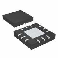
MAX1278ETC+ Maxim Integrated Products, MAX1278ETC+ Datasheet - Page 9

MAX1278ETC+
Manufacturer Part Number
MAX1278ETC+
Description
IC ADC 12BIT 1.8MSPS 12-TQFN
Manufacturer
Maxim Integrated Products
Datasheet
1.MAX1278ETC.pdf
(18 pages)
Specifications of MAX1278ETC+
Number Of Bits
12
Sampling Rate (per Second)
1.8M
Data Interface
MICROWIRE™, QSPI™, Serial, SPI™
Number Of Converters
1
Power Dissipation (max)
1.35W
Voltage Supply Source
Analog and Digital
Operating Temperature
-40°C ~ 85°C
Mounting Type
Surface Mount
Package / Case
12-WQFN Exposed Pad
Lead Free Status / RoHS Status
Lead free / RoHS Compliant
Figure 3. Functional Diagram
The MAX1276/MAX1278 use an input T/H and succes-
sive-approximation register (SAR) circuitry to convert
an analog input signal to a digital 12-bit output. The
serial interface requires only three digital lines (SCLK,
CNVST, and DOUT) and provides easy interfacing to
microprocessors (µPs) and DSPs. Figure 3 shows the
simplified internal structure for the MAX1276/MAX1278.
RGND
REF
AIN +
AIN -
Differential, 12-Bit ADCs with Internal Reference
5, 11
PIN
10
12
—
1
2
3
4
6
7
8
9
TRACK AND
HOLD
MAX1278
MAX1276
CNVST
NAME
RGND
DOUT
SCLK
GND
AIN+
4.096V
AIN-
N.C.
REF
V
_______________________________________________________________________________________
REF
V
EP
DD
1.8Msps, Single-Supply, Low-Power, True-
L
Detailed Description
12-BIT
SAR
ADC
V
DD
Negative Analog Input
Reference Voltage Output. Internal 4.096V reference output. Bypass REF with a 0.01µF capacitor and
a 4.7µF capacitor to RGND.
Reference Ground. Connect RGND to GND.
Positive Analog Supply Voltage (+4.75V to +5.25V). Bypass V
capacitor to GND.
No Connection
Ground. GND is internally connected to EP.
Positive Logic Supply Voltage (1.8V to V
to GND.
Serial Data Output. Data is clocked out on the rising edge of SCLK.
Convert Start. Forcing CNVST high prepares the part for a conversion. Conversion begins on the
falling edge of CNVST. The sampling instant is defined by the falling edge of CNVST.
Serial Clock Input. Clocks data out of the serial interface. SCLK also sets the conversion speed.
Positive Analog Input
Exposed Paddle. EP is internally connected to GND.
LOGIC AND
CONTROL
TIMING
OUTPUT
BUFFER
GND
V
L
CNVST
SCLK
DOUT
Figure 4. Equivalent Input Circuit
DD
). Bypass V
AIN+
AIN+
AIN-
AIN-
FUNCTION
L
with a 0.01µF capacitor and a 10µF capacitor
C
C
C
C
IN+
IN-
IN+
IN-
R
R
R
R
DD
IN+
IN-
IN+
IN-
HOLD/CONVERSION MODE
with a 0.01µF capacitor and a 10µF
ACQUISITION MODE
V
V
AZ
AZ
Pin Description
COMP
COMP
CAPACITIVE
CAPACITIVE
CONTROL
CONTROL
LOGIC
LOGIC
DAC
DAC
9


