MAX1031BEEG+ Maxim Integrated Products, MAX1031BEEG+ Datasheet
MAX1031BEEG+
Specifications of MAX1031BEEG+


Related parts for MAX1031BEEG+


MAX1031BEEG+ Summary of contents
Page 1
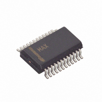
... System Supervision Data-Acquisition Systems Industrial Control Systems Patient Monitoring Data Logging Instrumentation AutoShutdown is a trademark of Maxim Integrated Products, Inc. SPI/QSPI are trademarks of Motorola, Inc. MICROWIRE is a trademark of National Semiconductor Corp. TOP VIEW AIN0 1 AIN1 2 ...
Page 2
ADCs with FIFO, Temp Sensor, Internal Reference ABSOLUTE MAXIMUM RATINGS V to GND ..............................................................-0.3V to +6V DD CS, SCLK, DIN, EOC, DOUT to GND.........-0. AIN0–AIN13, REF-/AIN_, CNVST/AIN_, REF+ to GND.........................................-0. Maximum Current into Any ...
Page 3
ELECTRICAL CHARACTERISTICS (continued +2.7V to +3.6V 300kHz SAMPLE noted. Typical values are +25°C.) A PARAMETER SYMBOL CONVERSION RATE Power-Up Time Acquisition Time Conversion Time t External Clock Frequency f SCLK Duty ...
Page 4
ADCs with FIFO, Temp Sensor, Internal Reference ELECTRICAL CHARACTERISTICS (continued +2.7V to +3.6V 300kHz SAMPLE noted. Typical values are +25°C.) A PARAMETER SYMBOL DIGITAL INPUTS (SCLK, DIN, , Input ...
Page 5
TIMING CHARACTERISTICS (Figure 1) PARAMETER SYMBOL SCLK Clock Period SCLK Duty Cycle SCLK Fall to DOUT Transition CS Rise to DOUT Disable CS Fall to DOUT Enable DIN to SCLK Rise Setup SCLK Rise to DIN Hold CS to SCLK ...
Page 6
ADCs with FIFO, Temp Sensor, Internal Reference (V = +3V +2.5V 4.8MHz REF SCLK SFDR vs. FREQUENCY 120 100 0 100 1000 FREQUENCY (kHz) SHUTDOWN ...
Page 7
V = +2.5V 4.8MHz REF SCLK INTERNAL REFERENCE VOLTAGE vs. TEMPERATURE 2.510 2.506 2.502 2.498 2.494 2.490 -40 - TEMPERATURE (°C) GAIN ERROR vs. SUPPLY VOLTAGE 0.6 0.4 0.2 0 ...
Page 8
ADCs with FIFO, Temp Sensor, Internal Reference MAX1031 MAX1031 MAX1029 MAX1027 TQFN QSOP 2–12, 26, 1–14 — 27, 28 — — 1–10 — — — — — — 11 — — — — — ...
Page 9
CS t CSS SCLK DIN t DOE DOUT Figure 1. Detailed Serial-Interface Timing Diagram CS DIN SCLK CNVST AIN1 AIN2 AIN15 REF- REF+ Figure 2. Functional Diagram _______________________________________________________________________________________ 10-Bit 300ksps ADCs with FIFO, Temp Sensor, Internal ...
Page 10
ADCs with FIFO, Temp Sensor, Internal Reference Detailed Description The MAX1027/MAX1029/MAX1031 are low-power, seri- al-output, multichannel ADCs with temperature-sensing capability for temperature-control, process-control, and monitoring applications. These 10-bit ADCs have inter- nal track and hold (T/H) circuitry that ...
Page 11
REF AIN0-AIN15 DAC GND (SINGLE ENDED); AIN0, AIN2, AIN4…AIN14 CIN+ (DIFFERENTIAL) HOLD GND CIN- (SINGLE ENDED); AIN1, AIN3, AIN5…AIN15 HOLD (DIFFERENTIAL Figure 3. Equivalent Input Circuit In differential mode, the T/H samples the difference between two analog ...
Page 12
ADCs with FIFO, Temp Sensor, Internal Reference temperature measurement is performed before the first temperature result is read out, the old measurement is overwritten by the new result. Temperature results are in degrees Celsius (two’s complement ...
Page 13
Table 2. Conversion Register* BIT BIT FUNCTION NAME — 7 (MSB) Set select conversion register. CHSEL3 6 Analog input channel select. CHSEL2 5 Analog input channel select. CHSEL1 4 Analog input channel select. CHSEL0 3 Analog input ...
Page 14
ADCs with FIFO, Temp Sensor, Internal Reference Table 3. Setup Register* BIT NAME BIT — 7 (MSB) Set to zero to select setup register. — 6 Set select setup register. Clock mode and CNVST configuration. ...
Page 15
Select scan mode 10 to scan the same channel multiple times. Clock mode 11 disables averaging. Write to the reset register (as shown in Table 7) to clear the FIFO or to reset all registers to their ...
Page 16
ADCs with FIFO, Temp Sensor, Internal Reference Table 6. Averaging Register* BIT NAME BIT — 7 (MSB) Set to zero to select averaging register. — 6 Set to zero to select averaging register. — 5 Set to 1 ...
Page 17
Internally Timed Acquisitions and Conversions Using CNVST Performing Conversions in Clock Mode 00 In clock mode 00, the wake up, acquisition, conversion, and shutdown sequences are initiated through CNVST and performed automatically using the internal oscilla- tor. Results are added ...
Page 18
ADCs with FIFO, Temp Sensor, Internal Reference CNVST (ACQUISITION1) (ACQUISITION2) CS (CONVERSION1) SCLK DOUT EOC REQUEST MULTIPLE CONVERSIONS BY SETTING CNVST LOW FOR EACH CONVERSION. Figure 5. Clock Mode 01 (CONVERSION BYTE) DIN CS SCLK DOUT EOC THE ...
Page 19
DIN (ACQUISITION1) CS SCLK DOUT EOC EXTERNALLY TIMED ACQUISITION, SAMPLING AND CONVERSION WITHOUT CNVST. Figure 7. Clock Mode 11 clock. Scanning and averaging are disabled, and the conversion result is available at DOUT during the con- version. See Figure 7 ...
Page 20
ADCs with FIFO, Temp Sensor, Internal Reference OUTPUT CODE FULL-SCALE TRANSITION 111 110 101 011 010 00 . ...
Page 21
TOP VIEW AIN0 1 AIN1 2 AIN2 3 AIN3 4 MAX1031 AIN4 5 AIN5 6 AIN6 7 AIN7 8 AIN8 9 AIN9 10 AIN10 11 AIN11 12 QSOP Effective Number of Bits Effective number of bits (ENOB) indicates the global ...
Page 22
... Maxim cannot assume responsibility for use of any circuitry other than circuitry entirely embodied in a Maxim product. No circuit patent licenses are implied. Maxim reserves the right to change the circuitry and specifications without notice at any time. 22 ____________________Maxim Integrated Products, 120 San Gabriel Drive, Sunnyvale, CA 94086 408-737-7600 © 2009 Maxim Integrated Products DESCRIPTION Maxim is a registered trademark of Maxim Integrated Products, Inc ...