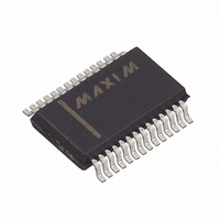
MAX117EAI+ Maxim Integrated Products, MAX117EAI+ Datasheet - Page 9

MAX117EAI+
Manufacturer Part Number
MAX117EAI+
Description
IC ADC 8BIT 400KSPS 28-SSOP
Manufacturer
Maxim Integrated Products
Datasheet
1.MAX113CAG.pdf
(12 pages)
Specifications of MAX117EAI+
Number Of Bits
8
Sampling Rate (per Second)
400k
Data Interface
Parallel
Number Of Converters
3
Power Dissipation (max)
762mW
Voltage Supply Source
Single Supply
Operating Temperature
-40°C ~ 85°C
Mounting Type
Surface Mount
Package / Case
28-SSOP
Lead Free Status / RoHS Status
Lead free / RoHS Compliant
Figure 6. Pipelined Mode Timing (WR = RD) (Mode = 1)
that contain the conversion result (D0–D7). INT also
goes low after the falling edge of RD and is reset on the
rising edge of RD or CS. The total conversion time is
therefore: t
Besides the two standard write-read-mode options,
“pipelined” operation can be achieved by connecting
WR and RD together (Figure 6). With CS low, driving
WR and RD low initiates a conversion and concurrently
reads the result of the previous conversion.
_____________Analog Considerations
Figures 7a, 7b, and 7c show typical reference connec-
tions. The voltages at REF+ and REF- set the ADC’s
analog input range (Figure 10). The voltage at REF-
defines the input that produces an output code of all
zeros, and the voltage at REF+ defines the input that
produces an output code of all ones.
The internal resistance from REF+ to REF- can be as
low as 1kΩ, and current will flow through it even when
the MAX113/MAX117 are shut down. Figure 7d shows
how an N-channel MOSFET can be connected to REF-
to break this current path during power-down. The FET
should have an on-resistance of less than 2Ω with a 3V
gate drive. When REF- is switched, as in Figure 7d, a
new conversion can be initiated after waiting a time
equal to the power-up delay (t
FET’s turn-on time.
Although REF+ is frequently connected to V
cuit of Figure 7d uses a low-current, low-dropout, 2.5V
voltage reference: the MAX872. Since the MAX872
cannot continuously furnish enough current for the ref-
RD, WR
A0–A2
D0–D7
INT
CS
OLD DATA (N - 1)
WR
ADDRESS
VALID (N)
t
ACQ
t
CSS
t
+ t
AH
RD
_______________________________________________________________________________________
t
WR
+ t
t
t
IHWR
CSH
ACC1
t
INTL
= 1800ns.
Pipelined Operation
UP
) plus the N-channel
8-Bit ADCs with 1µA Power-Down
t
ACQ
VALID (N + 1)
t
ID
ADDRESS
NEW DATA (N)
Reference
DD
, the cir-
+3V, 400ksps, 4/8-Channel,
erence resistance, this circuit is intended for applica-
tions where the MAX113/MAX117 are normally in stand-
by and are turned on in order to make measurements
at intervals greater than 100µs. C1 (the capacitor con-
nected to REF+) is slowly charged by the MAX872 dur-
ing the standby period, and furnishes the reference
current during the short measurement period.
The 4.7µF value of C1 ensures a voltage drop of less
than 1/2LSB when performing four to eight successive
conversions. Larger capacitors reduce the error still fur-
ther. Use ceramic or tantalum capacitors for C1.
Figure 7a. Power Supply as Reference
Figure 7b. External Reference, 2.5V Full Scale
Figure 7c. Input Not Referenced to GND
+3V
4.7µF
* CURRENT PATH MUST STILL
4.7µF
+3V
EXIST FROM V
4.7 F
+3V
0.1µF
IN-
0.1µF
TO GND
0.1 F
1
3
8
4
LM10
V
IN-
7
V
V
IN+
IN-
R*
6
2
+2.5V
V
V
V
0.1µF
IN+
IN-
IN+
34.8k
3.01k
+2.5V
IN_
GND
V
REF+
REF-
DD
0.1µF
MAX113
MAX117
0.1µF
IN_
GND
V
REF+
REF-
DD
V
REF+
REF-
DD
GND
MAX113
MAX117
MAX113
MAX117
IN_
9


