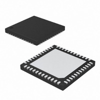
MAX19507ETM+ Maxim Integrated Products, MAX19507ETM+ Datasheet - Page 28

MAX19507ETM+
Manufacturer Part Number
MAX19507ETM+
Description
IC ADC 8BIT 2CH 130MSPS 48TQFN
Manufacturer
Maxim Integrated Products
Datasheet
1.MAX19507ETM.pdf
(35 pages)
Specifications of MAX19507ETM+
Number Of Bits
8
Sampling Rate (per Second)
130M
Data Interface
Serial, Parallel
Number Of Converters
2
Power Dissipation (max)
171mW
Voltage Supply Source
Analog and Digital
Operating Temperature
-40°C ~ 85°C
Mounting Type
Surface Mount
Package / Case
48-TQFN Exposed Pad
Lead Free Status / RoHS Status
Lead free / RoHS Compliant
Dual-Channel, 8-Bit, 130Msps ADC
Table 4. Data Timing Controls
Table 5. Data Timing Control Default
Settings
The MAX19507 features a dual CMOS, multiplexable,
reversible data bus. In parallel programming mode, con-
figure the data outputs (D0_–D7_) for offset binary, two’s
complement, or gray code using the FORMAT input.
Select multiplexed or dual-bus operation using the
OUTSEL input. See the Output Format register (01h) for
details on output formatting using the SPI interface. The
SPI interface offers additional flexibility where D0_–D7_
are reversed, so the LSB appears at D7_ and the MSB at
D0_. OVDD sets the output voltage; set OVDD between
1.8V and 3.3V. The digital outputs feature programmable
output impedance from 50Ω to 300Ω. Set the output
impedance for each bus using the CH_ Data Output
Termination Control registers (04h and 05h).
The MAX19507 provides programmable data timing con-
trol to allow for optimization of timing characteristics to
meet the system timing requirements. The timing adjust-
ment feature also allows for ADC performance improve-
ments by shifting the data output transition away from the
sampling instant. The data timing control signals are
summarized in Table 4. The default settings for timing
adjustment controls are given in Table 5. Many applica-
tions will not require adjustment from the default settings.
The effects of the data timing adjustment settings are
illustrated in Figures 13 and 14. The x axis is the sam-
pling rate and the y axis is the data delay in units of the
28
DCLKTIME<2:0>
DATA TIMING
DLY_HALF_T
DATA TIMING CONTROL
DTIME<2:0>
DA_BYPASS
CONTROL
______________________________________________________________________________________
DCLKTIME<2:0>
DLY_HALF_T
DA_BYPASS
DTIME<2:0>
DEFAULT
101
101
0
1
Programmable Data Timing
Data aligner active
T/2 Delay (3.85ns at 130Msps)
-T/16 (0.48ns at 130Msps)
-T/16 (0.48ns at 130Msps)
Data aligner bypass. When this control is active (high), data and DCLK delay is reduced by
approximately 3.4ns (relative to DA_BYPASS = 0).
When this control is active, data output is delayed by half clock period (T/2). This control does not
delay data output if MUX mode is active.
Allows adjustment of data output delay in T/16 increments, where T is the sample clock period.
Provides adjustment of DCLK delay in T/16 increments, where T is the sample clock period. When
DTIME and DCLKTIME are adjusted to the same setting, the rising edge of DCLK occurs T/8 prior
to data transitions.
DESCRIPTION
Digital Outputs
clock period. The solid lines are the nominal data timing
characteristics for the 14 available states of DTIME and
DLY_HALF_T. The heavy line represents the nominal
data timing characteristics for the default settings. Note
that the default timing adjustment setting for the
MAX19507 130Msps ADC results in an additional period
of data latency.
Tables 6 and 7 show the recommended timing control
settings versus sampling rate.
The nominal data timing characteristics versus sampling
rate for these recommended timing adjustment settings
are shown in Figures 15 and 16.
When DA_BYPASS = 1, the DCLKTIME delay setting
must be equal to or less than the DTIME delay setting, as
shown in Table 8.
The SHDN input (pin 7) toggles between any two power-
management states. The Power Management register
(00h) defines each power-management state. In default
state, SHDN = 1 shuts down the MAX19507 and SHDN =
0 returns to full power. Use of the SHDN input is not
required for power management. For either state of
SHDN, complete power-management flexibility is provid-
ed, including individual ADC channel power-manage-
ment control, through the Power Management register
(00h). The available reduced-power modes are shut-
down and standby. In standby mode, the reference and
duty-cycle equalizer circuits remain active for rapid
wake-up time. In standby mode, the externally applied
clock signal must remain active for the duty-cycle equal-
izer to remain locked. Typical wake-up time from standby
mode is 15µs. In shutdown mode, all circuits are turned
off except for the reference circuit required for the inte-
grated self-sensing voltage regulator. If the regulator is
active, there is additional supply current associated with
the regulator circuit when the device is in shutdown.
Typical wake-up time from shutdown mode is 5ms,
which is dominated by the RC time constant on REFIO.
DESCRIPTION
Power Management


