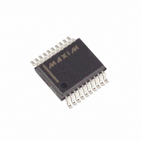
MAX1143ACAP+ Maxim Integrated Products, MAX1143ACAP+ Datasheet - Page 14

MAX1143ACAP+
Manufacturer Part Number
MAX1143ACAP+
Description
IC ADC 14BIT 200KSPS 20-SSOP
Manufacturer
Maxim Integrated Products
Datasheet
1.MAX1142BEAP.pdf
(20 pages)
Specifications of MAX1143ACAP+
Number Of Bits
14
Sampling Rate (per Second)
200k
Data Interface
MICROWIRE™, QSPI™, Serial, SPI™
Number Of Converters
1
Power Dissipation (max)
640mW
Voltage Supply Source
Analog and Digital
Operating Temperature
0°C ~ 70°C
Mounting Type
Surface Mount
Package / Case
20-SSOP
Lead Free Status / RoHS Status
Lead free / RoHS Compliant
14-Bit ADC, 200ksps, +5V Single-Supply
with Reference
An external reference can be placed at either the input
(REFADJ) or the output (REF) of the MAX1142/
MAX1143’s internal buffer amplifier.
When connecting an external reference to REFADJ, the
input impedance is typically 9kΩ. Using the buffered
REFADJ input makes buffering of the external reference
unnecessary. The internal buffer output must be
bypassed at REF with a 2.2µF capacitor.
When connecting an external reference at REF,
REFADJ must be connected to AV
ance at REF is 16kΩ for DC currents. During conver-
sion, an external reference at REF must deliver 250µA
DC load current and have an output impedance of 10Ω
or less. If the reference has a higher output impedance
or is noisy, bypass it at the REF pin with a 4.7µF capac-
itor.
The MAX1142/MAX1143 use a capacitive DAC that
provides an inherent track/hold function. Drive AIN with
a source impedance less than 10Ω. Any signal condi-
tioning circuitry must settle with 16-bit accuracy in less
than 500ns. Limit the input bandwidth to less than half
the sampling frequency to eliminate aliasing. The
MAX1142/MAX1143 has a complex input impedance
which varies from unipolar to bipolar mode (Figure 1).
The analog input range in unipolar mode is 0 to +12V
for the MAX1142, and 0 to +4.096V for the MAX1143. In
bipolar mode, the analog input can be -12V to +12V for
the MAX1142, and -4.096V to +4.096V for the
Table 3. Unipolar Full Scale and Zero Scale
Table 4. Bipolar Full Scale, Zero Scale, and Negative Scale
14
______________________________________________________________________________________
MAX1142
MAX1143
PART
MAX1142
MAX1143
PART
REFERENCE
External
External
Internal
Internal
DD
External reference
. The input imped-
REFERENCE
Analog Input
External
External
Internal
Internal
Input Range
NEGATIVE FULL
-12(V
-4.096V
SCALE
-V
REF
-12V
REF
/4.096)
MAX1143. Unipolar and bipolar mode is programmed
with the UNI/BIP bit of the Control-Byte. When using a
reference other than the MAX1142/MAX1143’s internal
+4.096V reference, the full-scale input range will vary
accordingly. The full-scale input range depends on the
voltage at REF and the sampling mode selected (Tables
3 and 4).
Clocking-in a Control-Byte starts input acquisition. In
bipolar mode, the main capacitor array starts acquiring
the input as soon as a start bit is recognized. If unipolar
mode is selected by the second DIN bit, the part will
immediately switch to unipolar sampling mode and
acquire a sample.
Acquisition can be extended by eight clock cycles by
setting M1 = 1, M0 = 1 (long acquisition mode). The
sampling instant in short acquisition completes on the
falling edge of the sixth clock cycle after the start bit
(Figure 2).
Figure 7. MAX1142 Reference-Adjust Circuit
ZERO SCALE
100k
+5V
0
0
0
0
24k
ZERO SCALE
0
0
0
0
510k
Input Acquisition and Settling
0.22 F
+12(V
FULL SCALE
+12(V
+4.096V
REFADJ
FULL SCALE
+V
+12V
MAX1142
REF
+4.096V
REF
+V
+12V
/4.096)
REF
REF
/4.096)


