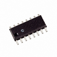
MCP3008-I/SL Microchip Technology, MCP3008-I/SL Datasheet - Page 15

MCP3008-I/SL
Manufacturer Part Number
MCP3008-I/SL
Description
IC ADC 10BIT 2.7V 8CH SPI 16SOIC
Manufacturer
Microchip Technology
Specifications of MCP3008-I/SL
Number Of Converters
1
Package / Case
16-SOIC (0.154", 3.90mm Width)
Number Of Bits
10
Sampling Rate (per Second)
200k
Data Interface
Serial, SPI™
Voltage Supply Source
Single Supply
Operating Temperature
-40°C ~ 85°C
Mounting Type
Surface Mount
Architecture
SAR
Conversion Rate
200 KSPs
Resolution
10 bit
Input Type
Voltage
Snr
200 dB
Maximum Operating Temperature
+ 85 C
Mounting Style
SMD/SMT
Minimum Operating Temperature
- 40 C
Package
16SOIC N
Sampling Rate
200 KSPS
Number Of Adcs
1
Number Of Analog Inputs
8|4
Digital Interface Type
Serial (4-Wire, SPI)
Polarity Of Input Voltage
Unipolar
Lead Free Status / RoHS Status
Lead free / RoHS Compliant
Lead Free Status / RoHS Status
Lead free / RoHS Compliant, Lead free / RoHS Compliant
Available stocks
Company
Part Number
Manufacturer
Quantity
Price
Company:
Part Number:
MCP3008-I/SL
Manufacturer:
MICROCHIP
Quantity:
2 100
Part Number:
MCP3008-I/SL
Manufacturer:
MICROCHI
Quantity:
20 000
5.0
Communication with the MCP3004/3008 devices is
accomplished using a standard SPI-compatible serial
interface. Initiating communication with either device is
done by bringing the CS line low (see Figure 5-1). If the
device was powered up with the CS pin low, it must be
brought high and back low to initiate communication.
The first clock received with CS low and D
constitute a start bit. The SGL/DIFF bit follows the start
bit and will determine if the conversion will be done
using single-ended or differential input mode. The next
three bits (D0, D1 and D2) are used to select the input
channel configuration. Table 5-1 and Table 5-2 show
the configuration bits for the MCP3004 and MCP3008,
respectively. The device will begin to sample the ana-
log input on the fourth rising edge of the clock after the
start bit has been received. The sample period will end
on the falling edge of the fifth clock following the start
bit.
Once the D0 bit is input, one more clock is required to
complete the sample and hold period (D
care” for this clock). On the falling edge of the next
clock, the device will output a low null bit. The next 10
clocks will output the result of the conversion with MSB
first, as shown in Figure 5-1. Data is always output from
the device on the falling edge of the clock. If all 10 data
bits have been transmitted and the device continues to
receive clocks while the CS is held low, the device will
output the conversion result LSB first, as is shown in
Figure 5-2. If more clocks are provided to the device
while CS is still low (after the LSB first data has been
transmitted), the device will clock out zeros indefinitely.
If necessary, it is possible to bring CS low and clock in
leading zeros on the D
often done when dealing with microcontroller-based
SPI ports that must send 8 bits at a time. Refer to
Section 6.1, “Using the MCP3004/3008 with Microcon-
troller (MCU) SPI Ports”, for more details on using the
MCP3004/3008 devices with hardware SPI ports.
2002 Microchip Technology Inc.
SERIAL COMMUNICATION
IN
line before the start bit. This is
IN
IN
is a “don’t
high will
TABLE 5-1:
TABLE 5-2:
* D2 is “don’t care” for MCP3004
Single/
Single
/Diff
Diff
1
1
1
1
1
1
1
1
0
0
0
0
0
0
0
0
1
1
1
1
0
0
0
0
Control Bit
Control Bit
Selections
Selections
D2* D1 D0
D2
0
0
0
0
1
1
1
1
0
0
0
0
1
1
1
1
X
X
X
X
X
X
X
X
D1 D0
MCP3004/3008
0
0
1
1
0
0
1
1
0
0
1
1
0
0
1
1
0
0
1
1
0
0
1
1
CONFIGURE BITS FOR THE
MCP3004
CONFIGURE BITS FOR THE
MCP3008
0
1
0
1
0
1
0
1
0
1
0
1
0
1
0
1
0
1
0
1
0
1
0
1
Configuration
Configuration
single-ended
single-ended
single-ended
single-ended
single-ended
single-ended
single-ended
single-ended
single-ended
single-ended
single-ended
single-ended
differential
differential
differential
differential
differential
differential
differential
differential
differential
differential
differential
differential
Input
Input
DS21295B-page 15
CH0 = IN+
CH1 = IN+
CH2 = IN+
CH3 = IN+
CH0 = IN+
CH1 = IN+
CH2 = IN+
CH3 = IN+
CH4 = IN+
CH5 = IN+
CH6 = IN+
CH7 = IN+
Selection
CH1 = IN-
CH0 = IN-
CH3 = IN-
CH2 = IN-
Selection
CH1 = IN-
CH0 = IN-
CH3 = IN-
CH2 = IN-
CH5 = IN-
CH4 = IN-
CH7 = IN-
CH6 = IN-
Channel
Channel
CH0
CH1
CH2
CH3
CH0
CH1
CH2
CH3
CH4
CH5
CH6
CH7


