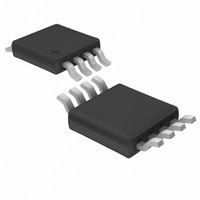
LTC1197LCMS8 Linear Technology, LTC1197LCMS8 Datasheet - Page 22

LTC1197LCMS8
Manufacturer Part Number
LTC1197LCMS8
Description
IC ADC 10BIT 250KHZ W/SD 8-MSOP
Manufacturer
Linear Technology
Datasheet
1.LTC1197CS8PBF.pdf
(28 pages)
Specifications of LTC1197LCMS8
Number Of Bits
10
Sampling Rate (per Second)
250k
Data Interface
MICROWIRE™, Serial, SPI™
Number Of Converters
1
Power Dissipation (max)
25mW
Voltage Supply Source
Single Supply
Operating Temperature
0°C ~ 70°C
Mounting Type
Surface Mount
Package / Case
8-TSSOP, 8-MSOP (0.118", 3.00mm Width)
Lead Free Status / RoHS Status
Contains lead / RoHS non-compliant
Available stocks
Company
Part Number
Manufacturer
Quantity
Price
Company:
Part Number:
LTC1197LCMS8
Manufacturer:
LT
Quantity:
10 000
Part Number:
LTC1197LCMS8
Manufacturer:
LINEAR/凌特
Quantity:
20 000
Part Number:
LTC1197LCMS8#TRPBF
Manufacturer:
LINEAR/凌特
Quantity:
20 000
LTC1197/LTC1197L
LTC1199/LTC1199L
TYPICAL APPLICATIO S
22
LOCATION A + 1
Hardware and Software Interface to Motorola MC68HC05C4
LOCATION A
ANALOG
INPUTS
MPU TRANSMIT
MPU RECEIVED
D
OUT
WORD
WORD
B7
0
D
CLK
OUT
from LTC1199 Stored in MC68HC05C4
D
CS
IN
B6
0
LTC1199
B5
0
D
CLK
OUT
B4
D
0
CS
IN
START
BIT
START
1
?
B3
0
SGL/
DIFF
SGL/
?
DIFF
U
B2
0
ODD/
SIGN
Data Exchange Between LTC1199 and MC68HC05C4
ODD/
SIGN
?
MSB
B9
B1
1ST TRANSFER
DUMMY
SCK
MISO
MOSI
C0
1197/99 TA05
DUMMY
MC68HC05C4
?
BYTE 1
B8
B0
LSB
X
0
BYTE 1
BYTE 2
1197/99 TA04
B9
X
0
B8
B9
X
B8
X
B7
LABEL
START
B6
X
B7
DON‘T CARE
MNEMONIC
BCLRn
LDA
STA
TST
BPL
LDA
STA
AND
STA
TST
BPL
BSETn
LDA
STA
B5
B6
X
B4
B5
X
BYTE 2 (DUMMY)
X = DON‘T CARE
2ND TRANSFER
B3
B4
X
B2
Bit 0 Port C goes low (CS goes low)
Load LTC1199 D
Load LTC1199 D
Transfer begins
Test status of SPIF
Loop to previous instruction if not done
with transfer
Load contents of SPI data register
into ACC (D
Start next SPI cycle
Clear 6 MSBs of the first D
Store in memory location A (MSBs)
Test status of SPIF
Loop to previous instruction if not done
with transfer
Set B0 of Port C (CS goes high)
Load contents of SPI data register into
ACC. (D
Store in memory location A + 1 (LSBs)
B3
X
B1
B2
X
OUT
B0
OUT
LSBs)
B1
X
MSBs)
IN
IN
COMMENTS
B0
X
word into ACC
word into SPI from ACC
OUT
1197/99 TA03
word


