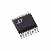
LTC2435-1CGN#PBF Linear Technology, LTC2435-1CGN#PBF Datasheet - Page 13

LTC2435-1CGN#PBF
Manufacturer Part Number
LTC2435-1CGN#PBF
Description
IC ADC DIFF I/REF 20BIT 16-SSOP
Manufacturer
Linear Technology
Datasheet
1.LTC2435-1CGN.pdf
(40 pages)
Specifications of LTC2435-1CGN#PBF
Number Of Bits
20
Sampling Rate (per Second)
13.75
Data Interface
MICROWIRE™, Serial, SPI™
Number Of Converters
2
Power Dissipation (max)
1mW
Voltage Supply Source
Single Supply
Operating Temperature
0°C ~ 70°C
Mounting Type
Surface Mount
Package / Case
16-SSOP (0.150", 3.90mm Width)
Lead Free Status / RoHS Status
Lead free / RoHS Compliant
Available stocks
Company
Part Number
Manufacturer
Quantity
Price
APPLICATIO S I FOR ATIO
The LTC2435/LTC2435-1 perform a full-scale calibration
every conversion cycle. This calibration is transparent to
the user and has no effect on the cyclic operation de-
scribed above. The advantage of continuous calibration is
extreme stability of full-scale readings with respect to time,
supply voltage change and temperature drift.
Unlike the LTC2430, the LTC2435 and LTC2435-1 do not
perform an offset calibration every conversion cycle. This
enables the LTC2435/LTC2435-1 to double their output
rate while maintaining line frequency rejection. The initial
offset of the LTC2435/LTC2435-1 is within 5mV indepen-
dent of V
lator architecture, the temperature drift of the offset is less
than 100nV/°C. More information on the LTC2435/
LTC2435-1 offset is described in the Offset Accuracy and
Drift section of this data sheet.
Power-Up Sequence
The LTC2435/LTC2435-1 automatically enter an internal
reset state when the power supply voltage V
below approximately 2.2V. This feature guarantees the
integrity of the conversion result and of the serial interface
mode selection. (See the 2-wire I/O sections in the Serial
Interface Timing Modes section.)
When the V
the converter creates an internal power-on-reset (POR)
signal with a duration of approximately 1ms. The POR
signal clears all internal registers. Following the POR
signal, the LTC2435/LTC2435-1 start a normal conversion
cycle and follow the succession of states described above.
The first conversion result following POR is accurate
within the specifications of the device if the power supply
voltage is restored within the operating range (2.7V to
5.5V) before the end of the POR time interval.
Reference Voltage Range
These converters accept a truly differential external refer-
ence voltage. The absolute/common mode voltage speci-
fication for the REF
from GND to V
REF
+
pin must always be more positive than the REF
REF
. Based on the LTC2435/LTC2435-1 new modu-
CC
voltage rises above this critical threshold,
CC
. For correct converter operation, the
+
U
and REF
U
–
pins covers the entire range
W
U
CC
drops
–
pin.
The LTC2435/LTC2435-1 can accept a differential refer-
ence voltage from 0.1V to V
is determined by the thermal noise of the front-end cir-
cuits, and as such, its value is nearly constant with
reference voltage. A decrease in reference voltage will not
significantly improve the converter’s effective resolution.
On the other hand, a reduced reference voltage will im-
prove the converter’s overall INL performance. A reduced
reference voltage will also improve the converter perfor-
mance when operated with an external conversion clock
(external F
rates (see the Output Data Rate section).
Input Voltage Range
The analog input is truly differential with an absolute/
common mode range for the IN
extending from GND – 0.3V to V
these limits, the ESD protection devices begin to turn on
and the errors due to input leakage current increase
rapidly. Within these limits, the LTC2435/LTC2435-1 con-
vert the bipolar differential input signal, V
from – FS = – 0.5 • V
REF
the overrange or the underrange condition using distinct
output codes.
Input signals applied to IN
300mV below ground and above V
fault current, resistors of up to 5k may be added in series
with the IN
mance of the device. In the physical layout, it is important
to maintain the parasitic capacitance of the connection
between these series resistors and the corresponding pins
as low as possible; therefore, the resistors should be
located as close as practical to the pins. The effect of the
series resistance on the converter accuracy can be evalu-
ated from the curves presented in the Input Current/
Reference Current sections. In addition, series resistors
will introduce a temperature dependent offset error due to
the input leakage current. A 1nA input leakage current will
develop a 1ppm offset error on a 5k resistor if V
This error has a very strong temperature dependency.
+
– REF
O
–
+
. Outside this range, the converters indicate
signal) at substantially higher output data
and IN
LTC2435/LTC2435-1
REF
–
pins without affecting the perfor-
to +FS = 0.5 • V
+
CC
and IN
. The converter output noise
CC
+
–
CC
. In order to limit any
and IN
pins may extend by
REF
+ 0.3V. Outside
IN
where V
–
= IN
input pins
REF
+
13
– IN
= 5V.
REF
24351fb
–
=
,


