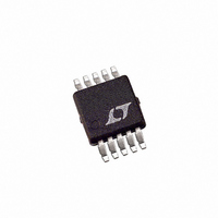
LTC1407CMSE Linear Technology, LTC1407CMSE Datasheet - Page 3

LTC1407CMSE
Manufacturer Part Number
LTC1407CMSE
Description
IC ADC 12BIT 3MSPS SAMPLE 10MSOP
Manufacturer
Linear Technology
Datasheet
1.LTC1407CMSEPBF.pdf
(24 pages)
Specifications of LTC1407CMSE
Number Of Bits
12
Sampling Rate (per Second)
3M
Data Interface
Serial, SPI™
Number Of Converters
1
Power Dissipation (max)
14mW
Voltage Supply Source
Single Supply
Operating Temperature
0°C ~ 70°C
Mounting Type
Surface Mount
Package / Case
10-TFSOP, 10-MSOP (0.118", 3.00mm Width) Exposed Pad
Lead Free Status / RoHS Status
Contains lead / RoHS non-compliant
Available stocks
Company
Part Number
Manufacturer
Quantity
Price
Company:
Part Number:
LTC1407CMSE
Manufacturer:
LT
Quantity:
10 000
Part Number:
LTC1407CMSE
Manufacturer:
LINEAR/凌特
Quantity:
20 000
Company:
Part Number:
LTC1407CMSE#PBF
Manufacturer:
LT
Quantity:
214
Part Number:
LTC1407CMSE#PBF
Manufacturer:
LINEAR/凌特
Quantity:
20 000
Company:
Part Number:
LTC1407CMSE#TRPBF
Manufacturer:
LT
Quantity:
4 390
Company:
Part Number:
LTC1407CMSE-1
Manufacturer:
LT
Quantity:
10 000
Part Number:
LTC1407CMSE-1#PBF
Manufacturer:
LT凌特厂
Quantity:
20 000
Company:
Part Number:
LTC1407CMSE-1#TRPBF
Manufacturer:
LT
Quantity:
560
DYNAMIC ACCURACY
INTERNAL REFERENCE CHARACTERISTICS
ANALOG INPUT
otherwise specifi cations are at T
SYMBOL PARAMETER
V
V
I
C
t
t
t
t
CMRR
otherwise specifi cations are at T
SYMBOL PARAMETER
SINAD
THD
SFDR
IMD
PARAMETER
V
V
V
V
V
IN
ACQ
AP
JITTER
SK
IN
CM
IN
REF
REF
REF
REF
REF
Output Voltage
Output Tempco
Line Regulation
Output Resistance
Setting Time
Signal-to-Noise Plus
Distortion Ratio
Total Harmonic
Distortion
Spurious Free
Dynamic Range
Intermodulation
Distortion
Code-to-Code
Transition Noise
Full Power Bandwidth
Full Linear Bandwidth
Analog Differential Input Range (Notes 3, 9)
Analog Common Mode + Differential
Input Range (Note 10)
Analog Input Leakage Current
Analog Input Capacitance
Sample-and-Hold Acquisition Time
Sample-and-Hold Aperture Delay Time
Sample-and-Hold Aperture Delay Time Jitter
Sample-and-Hold Aperture Skew from CH0 to CH1
Analog Input Common Mode Rejection Ratio
CONDITIONS
100kHz Input Signal
750kHz Input Signal
750kHz Input Signal (H Grade)
100kHz Input Signal, External V
750kHz Input Signal, External V
100kHz First 5 Harmonics
750kHz First 5 Harmonics
750kHz First 5 Harmonics (H Grade)
100kHz Input Signal
750kHz Input Signal
1.25V to 2.5V 1.40MHz into CH0
1.56MHz into CH0
V
V
S/(N + D) ≥ 68dB
The
A
A
REF
IN
= 25°C. With internal reference, V
= 25°C. With internal reference, V
= 2.5V
= 2.5V (Note 17)
l
denotes the specifi cations which apply over the full operating temperature range,
P-P
The
, SDO = 11585LSB
l
–
. Also Applicable to CH1
denotes the specifi cations which apply over the full operating temperature range,
CONDITIONS
I
V
Load Current = 0.5mA
OUT
DD
CONDITIONS
2.7V ≤ V
(Note 6)
f
f
= 2.7V to 3.6V, V
= 0
IN
IN
= 1MHz, V
= 100MHz, V
REF
REF
P-P
+
, 0V to 1.25V,
= 3.3V, V
= 3.3V, V
(–3dBFS) (Note 15)
DD
≤ 3.3V
IN
DD
DD
+
DD
DD
= 0V to 3V
IN
and CH1
REF
= 3V.
= 3V.
= 0V to 3V
≥ 3.3V
≥ 3.3V
= 2.5V
T
–
A
= 25°C. V
l
l
l
l
MIN
LTC1407/LTC1407H
68
67
DD
LTC1407/LTC1407A
= 3V.
70.5
70.5
70.5
72.0
72.0
0.25
TYP
–87
–83
–82
–82
87
83
50
5
l
l
MIN
MAX
–77
–76
MIN
LTC1407A/LTC1407AH
MIN
TYP
600
2.5
0.2
70
69
15
2
0 to V
0 to 2.5
TYP
200
–60
–15
0.3
13
1
73.5
73.5
73.5
76.3
76.3
DD
TYP
–90
–86
–85
–82
90
86
50
1
5
MAX
MAX
39
MAX
1
–80
–79
LSB
ppm/°C
UNITS
UNITS
UNITS
1407fb
3
μV/V
MHz
MHz
RMS
ms
dB
dB
dB
dB
dB
dB
dB
dB
dB
dB
dB
μA
dB
dB
pF
ns
ns
ps
ps
Ω
V
V
V


