LTC2439-1IGN#TR Linear Technology, LTC2439-1IGN#TR Datasheet - Page 9

LTC2439-1IGN#TR
Manufacturer Part Number
LTC2439-1IGN#TR
Description
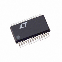
IC ADC 16BIT 16CH MCRPWR 28SSOP
Manufacturer
Linear Technology
Datasheet
1.LTC2439-1CGN.pdf
(28 pages)
Specifications of LTC2439-1IGN#TR
Number Of Bits
16
Sampling Rate (per Second)
6.8
Data Interface
MICROWIRE™, Serial, SPI™
Number Of Converters
1
Power Dissipation (max)
1mW
Voltage Supply Source
Single Supply
Operating Temperature
-40°C ~ 85°C
Mounting Type
Surface Mount
Package / Case
28-SSOP (0.150", 3.95mm Width)
Lead Free Status / RoHS Status
Contains lead / RoHS non-compliant
Available stocks
Company
Part Number
Manufacturer
Quantity
Price
APPLICATIO S I FOR ATIO
Conversion Clock
A major advantage the delta-sigma converter offers over
conventional type converters is an on-chip digital filter
(commonly implemented as a Sinc or Comb filter). For
high resolution, low frequency applications, this filter is
typically designed to reject line frequencies of 50Hz and
60Hz plus their harmonics. The filter rejection perfor-
mance is directly related to the accuracy of the converter
system clock. The LTC2439-1 incorporates a highly accu-
rate on-chip oscillator. This eliminates the need for exter-
nal frequency setting components such as crystals or
oscillators. Clocked by the on-chip oscillator, the
LTC2436-1 achieves a minimum of 87dB rejection over
the range 49Hz to 61.2Hz.
Ease of Use
The LTC2439-1 data output has no latency, filter settling
delay or redundant data associated with the conversion
cycle. There is a one-to-one correspondence between the
conversion and the output data. Therefore, multiplexing
multiple analog voltages is easy.
The LTC2439-1 performs offset and full-scale calibrations
in every conversion cycle. This calibration is transparent to
the user and has no effect on the cyclic operation described
above. The advantage of continuous calibration is extreme
stability of offset and full-scale readings with respect to time,
supply voltage change and temperature drift.
Power-Up Sequence
The LTC2439-1 automatically enters an internal reset state
when the power supply voltage V
mately 2V. This feature guarantees the integrity of the
conversion result and of the serial interface mode selec-
tion. (See the 3-wire I/O sections in the Serial Interface
Timing Modes section.)
When the V
the converter creates an internal power-on-reset (POR)
signal with a typical duration of 1ms. The POR signal
clears all internal registers. Following the POR signal,
the LTC2439-1 starts a normal conversion cycle and
follows the succession of states described above. The first
conversion result following POR is accurate within the
CC
voltage rises above this critical threshold,
U
U
CC
W
drops below approxi-
U
specifications of the device if the power supply voltage is
restored within the operating range (2.7V to 5.5V) before
the end of the POR time interval.
Reference Voltage Range
The LTC2439-1 accepts a truly differential external refer-
ence voltage. The absolute/common mode voltage speci-
fication for the REF
from GND to V
REF
The LTC2439-1 can accept a differential reference voltage
from 0.1V to V
mined by the thermal noise of the front-end circuits, and
as such, its value in microvolts is nearly constant with
reference voltage. A decrease in reference voltage will
significantly improve the converter’s effective resolution,
since the thermal noise (1µV) is well below the quantiza-
tion level of the device (75.6µV for a 5V reference). At the
minimum reference (100mV) the thermal noise
remains constant at 1µV RMS (or 6µV
quantization is reduced to 1.5µV per LSB. As a result,
lowering the reference improves the effective resolution
for low level input voltages.
Input Voltage Range
The two selected pins are labeled IN
Once selected (either differential or single-ended multiplex-
ing mode), the analog input is differential with a common
mode range for the IN
GND – 0.3V to V
protection devices begin to turn on and the errors due to
input leakage current increase rapidly. Within these limits,
the LTC2439-1 converts the bipolar differential input sig-
nal, V
• V
converter indicates the overrange or the underrange con-
dition using distinct output codes.
Input signals applied to IN
300mV below ground or above V
fault current, resistors of up to 5k may be added in series
with the IN
of the device. In the physical layout, it is important to
REF
+
pin must always be more positive than the REF
IN
where V
= IN
+
or IN
+
– IN
REF
CC
CC
CC
–
. The converter output noise is deter-
. For correct converter operation, the
–
pins without affecting the performance
+
= REF
, from – FS = – 0.5 • V
+ 0.3V. Outside these limits, the ESD
and REF
+
and IN
+
– REF
+
–
pins covers the entire range
–
and IN
input pins extending from
–
CC
. Outside this range the
+
. In order to limit any
LTC2439-1
and IN
–
pins may extend
REF
P-P
–
(see Table 1).
), while the
to +FS = 0.5
–
24391fa
pin.
9


