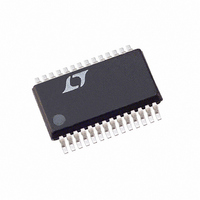
LTC2424IG Linear Technology, LTC2424IG Datasheet - Page 20

LTC2424IG
Manufacturer Part Number
LTC2424IG
Description
IC ADC 20BIT 4CH MICROPWR 28SSOP
Manufacturer
Linear Technology
Datasheet
1.LTC2424CGPBF.pdf
(36 pages)
Specifications of LTC2424IG
Number Of Bits
20
Sampling Rate (per Second)
7.5
Data Interface
MICROWIRE™, Serial, SPI™
Number Of Converters
1
Power Dissipation (max)
1mW
Voltage Supply Source
Single Supply
Operating Temperature
-40°C ~ 85°C
Mounting Type
Surface Mount
Package / Case
28-SSOP (0.200", 5.30mm Width)
Lead Free Status / RoHS Status
Contains lead / RoHS non-compliant
Available stocks
Company
Part Number
Manufacturer
Quantity
Price
Part Number:
LTC2424IG#PBF
Manufacturer:
LINEAR/凌特
Quantity:
20 000
Part Number:
LTC2424IG#TRPBF
Manufacturer:
LINEAR/凌特
Quantity:
20 000
APPLICATIONS
LTC2424/LTC2428
External Serial Clock (SPI/MICROWIRE Compatible)
This timing mode uses an external serial clock (SCK) to
shift out the conversion result, see Figure 13. This same
external clock signal drives the CLK pin in order to pro-
gram the multiplexer. A single CS signal drives both the
multiplexer CSMUX and converter CSADC inputs. This
common signal is used to monitor and control the state of
the conversion as well as enable the channel selection.
The serial clock mode is selected on the falling edge of
CSADC. To select the external serial clock mode, the serial
clock pin (SCK) must be LOW during each CSADC falling
edge.
The serial data output pin (SDO) is Hi-Z as long as CSADC
is HIGH. At any time during the conversion cycle, CSADC
may be pulled LOW in order to monitor the state of the
converter. While CSADC is LOW, EOC is output to the SDO
pin. EOC = 1 while a conversion is in progress and EOC =
0 if the device is in the sleep state. Independent of CSADC,
the device automatically enters the sleep state once the
conversion is complete. While the device is in the sleep
state and CSADC is HIGH, the power consumption is
reduced an order of magnitude.
20
SCK/CLK
CSADC/
CSMUX
SDO
D
IN
TEST EOC
DON’T CARE
Hi-Z
TEST EOC
U
EN
INFORMATION
U
D2
D1
Hi-Z
D0
W
Figure 13. External Serial Clock Timing Diagram
TO 1.12V
–0.12V
U
TO V
2.7V TO 5.5V
BIT23
0.1V
REF
REF
CC
BIT22
V
FS
CH0
TO CH7
MUXOUT
ADCIN
ZS
GND
LTC2424/LTC2428
CC
SET
SET
BIT21
SIG
While the device is in the sleep state, prior to entering the
data output state, the user may program the multiplexer.
As shown in Figure 13, the multiplexer channel is selected
by serial shifting a 4-bit word into the D
edge of CLK (CLK is tied to SCK). The first bit is an enable
bit that must be HIGH in order to program a channel. The
next three bits determine which channel is selected, see
Table 3. On the falling edge of CSMUX, the new channel is
selected and will be valid for the first conversion per-
formed following the data output state. Clock signals ap-
plied to the CLK pin while CSMUX is LOW (during the data
output state) will have no effect on the channel selection.
Furthermore, if D
the sleep state, the channel selection is unchanged.
When the device is in the sleep state (EOC = 0), its
conversion result is held in an internal static shift register.
The device remains in the sleep state until the first rising
edge of SCK is seen while CSADC is LOW. Data is shifted
out the SDO pin on each falling edge of SCK. This enables
external circuitry to latch the output on the rising edge of
SCK. EOC can be latched on the first rising edge of SCK
and the last bit of the conversion result can be latched on
BIT20
EXR
CSMUX
CSADC
SDO
SCK
CLK
BIT19 BIT18
D
MSB
F
IN
O
CS
SCK
DON’T CARE
V
CC
= 50Hz REJECTION
= EXTERNAL OSCILLATOR
= 60Hz REJECTION
IN
is held LOW or CLK is held LOW during
BIT4
BIT0
LSB
IN
pin on the rising
Hi-Z
TEST EOC
24248 F13


