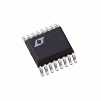
LTC2415-1IGN#TR Linear Technology, LTC2415-1IGN#TR Datasheet - Page 28

LTC2415-1IGN#TR
Manufacturer Part Number
LTC2415-1IGN#TR
Description
IC ADC 24BIT DIFFINPUT/REF16SSOP
Manufacturer
Linear Technology
Datasheet
1.LTC2415CGNPBF.pdf
(40 pages)
Specifications of LTC2415-1IGN#TR
Number Of Bits
24
Sampling Rate (per Second)
13.75
Data Interface
MICROWIRE™, Serial, SPI™
Number Of Converters
2
Power Dissipation (max)
1mW
Voltage Supply Source
Single Supply
Operating Temperature
-40°C ~ 85°C
Mounting Type
Surface Mount
Package / Case
16-SSOP (0.150", 3.90mm Width)
Lead Free Status / RoHS Status
Contains lead / RoHS non-compliant
Other names
LTC2415-1IGNTR
Available stocks
Company
Part Number
Manufacturer
Quantity
Price
LTC2415/LTC2415-1
APPLICATIO S I FOR ATIO
For relatively small values of input capacitance (C
0.01 F), the voltage on the sampling capacitor settles
almost completely and relatively large values for the
source impedance result in only small errors. Such values
for C
performance without significant benefits of signal filtering
and the user is advised to avoid them. Nevertheless, when
small values of C
of input multiplexers, wires, connectors or sensors, the
LTC2415/LTC2415-1 can maintain their exceptional accu-
racy while operating with relative large values of source
resistance as shown in Figures 20 and 21. These mea-
sured results may be slightly different from the first order
approximation suggested earlier because they include the
effect of the actual second order input network together
with the nonlinear settling process of the input amplifiers.
For small C
almost independently and there is little benefit in trying to
match the source impedance for the two pins.
Larger values of input capacitors (C
required in certain configurations for antialiasing or gen-
eral input signal filtering. Such capacitors will average the
input sampling charge and the external source resistance
will see a quasi constant input differential impedance.
When F
typical differential input resistance is 1.8M (LTC2415),
1.97M (LTC2415-1) which will generate a gain error of
approximately 0.28ppm for each ohm of source resis-
tance driving IN
(internal oscillator and 50Hz notch), the typical differential
input resistance is 2.16M
error of approximately 0.23ppm for each ohm of source
resistance driving IN
external oscillator with a frequency f
sion clock operation), the typical differential input resis-
tance is 0.28 • 10
source resistance driving IN
1.78 • 10
resistance on the two input pins is additive with respect to
this gain error. The typical +FS and –FS errors as a function
of the sum of the source resistance seen by IN
large values of C
28
IN
O
will deteriorate the converter offset and gain
–6
= LOW (internal oscillator and 60Hz notch), the
• f
IN
EOSC
values, the settling on IN
+
or IN
IN
IN
ppm gain error. The effect of the source
are shown in Figures 22 and 23.
are unavoidably present as parasitics
U
+
–
. For the LTC2415, when F
12
or IN
/f
U
EOSC
–
which will generate a gain
. When F
+
or IN
EOSC
W
and each ohm of
IN
> 0.01 F) may be
O
+
(external conver-
–
and IN
is driven by an
will result in
+
and IN
U
O
–
= HIGH
occurs
–
IN
for
<
In addition to this gain error, an offset error term may also
appear. The offset error is proportional to the mismatch
between the source impedance driving the two input pins
IN
reference common mode voltages. While the input drive
circuit nonzero source impedance combined with the
converter average input current will not degrade the INL
performance, indirect distortion may result from the modu-
lation of the offset error by the common mode component
of the input signal. Thus, when using large C
values, it is advisable to carefully match the source imped-
ance seen by the IN
(internal oscillator and 60Hz notch), every 1 mismatch
in source impedance transforms a full-scale common
mode input signal into a differential mode input signal of
0.28ppm. When F
notch), every 1 mismatch in source impedance trans-
forms a full-scale common mode input signal into a
differential mode input signal of 0.23ppm. When F
driven by an external oscillator with a frequency f
every 1
full-scale common mode input signal into a differential
mode input signal of 1.78 • 10
shows the typical offset error due to input common mode
voltage for various values of source resistance imbalance
between the IN
used.
If possible, it is desirable to operate with the input signal
common mode voltage very close to the reference signal
common mode voltage as is the case in the ratiometric
measurement of a symmetric bridge. This configuration
eliminates the offset error caused by mismatched source
impedances.
The magnitude of the dynamic input current depends upon
the size of the very stable internal sampling capacitors and
upon the accuracy of the converter sampling clock. The
accuracy of the internal clock over the entire temperature
and power supply range is typical better than 0.5%. Such
a specification can also be easily achieved by an external
clock. When relatively stable resistors (50ppm/ C) are
+
and IN
–
mismatch in source impedance transforms a
and with the difference between the input and
+
and IN
O
= HIGH (internal oscillator and 50Hz
+
and IN
–
pins when large C
–
–6
pins. When F
• f
EOSC
ppm. Figure 24
IN
IN
values are
O
sn2415 24151fs
capacitor
= LOW
EOSC
O
is
,


