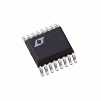
LTC1402IGN Linear Technology, LTC1402IGN Datasheet - Page 12

LTC1402IGN
Manufacturer Part Number
LTC1402IGN
Description
IC ADC 12BIT 2.2MSPS SHDN 16SSOP
Manufacturer
Linear Technology
Datasheet
1.LTC1402CGNPBF.pdf
(24 pages)
Specifications of LTC1402IGN
Number Of Bits
12
Sampling Rate (per Second)
2.2M
Data Interface
MICROWIRE™, Serial, SPI™
Number Of Converters
1
Power Dissipation (max)
150mW
Voltage Supply Source
Analog and Digital, Dual ±
Operating Temperature
-40°C ~ 85°C
Mounting Type
Surface Mount
Package / Case
16-SSOP (0.150", 3.90mm Width)
Lead Free Status / RoHS Status
Contains lead / RoHS non-compliant
Available stocks
Company
Part Number
Manufacturer
Quantity
Price
Company:
Part Number:
LTC1402IGN
Manufacturer:
NEC
Quantity:
6 945
Part Number:
LTC1402IGN#PBF
Manufacturer:
LINEAR/凌特
Quantity:
20 000
Part Number:
LTC1402IGN#TRPBF
Manufacturer:
LINEAR/凌特
Quantity:
20 000
APPLICATIONS
LTC1402
INTERNAL REFERENCE
The LTC1402 has an on-chip, temperature compensated,
curvature corrected, bandgap reference that is factory
trimmed to 2.048V. It is connected internally to a reference
amplifier, see Figure 4. The reference amplifier amplifies
the voltage at the V
internal reference voltage of 4.096V. This provides buffer-
ing for the high speed capacitive DAC. The reference
amplifier output V
capacitor to ground. The reference amplifier is stable with
capacitors of 1 F or greater. For the best noise perfor-
mance, a 10 F ceramic or a 10 F tantalum in parallel with
a 0.1 F ceramic is recommended.
The V
shown in Figure 5a. The GAIN pin (Pin 7) is tied to the
positive supply to disable the internal reference buffer.
A DAC may also be used to drive V
Figure 6. This is useful in applications where the peak
input signal amplitude may vary. The input span of the
12
Figure 5a. Using the LT1019-2.5 as an External Reference
REF
4.096V
LT1019-2.5
pin can be driven with an external reference as
V
10 F
5V
IN
Figure 4. LTC1402 Reference Circuit
5
7
6
V
OUT
V
GAIN
AGND2
LTC1402
REF
REF
U
REF
64k
, (Pin 5) must be bypassed with a
ANALOG INPUT
REFERENCE
64k
pin by 2 to create the required
5V
INFORMATION
AMP
U
10 F
+
–
2.048V
3
4
5
6
7
W
A
A
V
AGND2
GAIN
IN
IN
REF
REFERENCE
+
–
BANGAP
REF
LTC1402
as shown in
1402 F04
1402 F04a
U
ADC can then be adjusted to match the peak input signal,
maximizing the signal-to-noise ratio. The filtering of the
internal LTC1402 reference amplifier will limit the band-
width and settling time of this circuit. A settling time of
5ms should be allowed after a reference adjustment.
DIFFERENTIAL INPUTS
The LTC1402 has a unique differential sample-and-hold
circuit that allows inputs from –2.5V to 5V. The ADC will
always convert the difference of A
of the common mode voltage. The common mode rejec-
tion holds up at extremely high frequencies, see Figure 7.
The only requirement is that both inputs not exceed
– 2.5V or 5V. Integral nonlinearity errors (INL) and differ-
ential nonlinearity errors (DNL) are independent of the
common mode voltage. However, the bipolar zero error
(BZE) will vary. The change in BZE is typically less than
0.1% of the common mode voltage. Figure 5b shows the
use of bipolar mode with single 5V supply.
LT1019-2.5
Figure 6. Driving V
Figure 5b. Bipolar Mode with Single Supply
V
5V
IN
LTC1451
2.5V
2.5V 2.048V
ANALOG INPUT
10 F
REF
5V
10 F
with a 12 Bit, V
V
IN
10 F
3
4
5
6
7
IN
3
4
5
6
7
+
A
A
V
AGND2
GAIN
IN
IN
REF
– A
A
A
V
AGND2
GAIN
+
–
IN
IN
REF
LTC1402
+
–
IN
LTC1402
OUT
–
independent
DAC
1402 F04a
V
BIP
SS
1402 F06
14
8
5V


