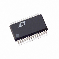
LTC1412IG Linear Technology, LTC1412IG Datasheet

LTC1412IG
Specifications of LTC1412IG
Available stocks
Related parts for LTC1412IG
LTC1412IG Summary of contents
Page 1
... Bipolar Input Range No Pipeline Delay 28-Pin SSOP Package U APPLICATIONS Telecommunications Digital Signal Processing Mulitplexed Data Acquisition Systems High Speed Data Acquisition Spectrum Analysis Imaging Systems , LTC and LT are registered trademarks of Linear Technology Corporation. U TYPICAL APPLICATION 10 F LTC1412 + A IN S/H 12-BIT ADC – ...
Page 2
... With internal reference (Notes 5, 6) CONDITIONS (Note 7) (Note OUT(REF) CONDITIONS 4.75V V 5.25V, – 5.25V High Between Conversions During Conversions – – 2.5V < < 2. INFORMATION ORDER PART TOP VIEW NUMBER LTC1412CG LTC1412IG 4 25 BUSY CONVST 7 OGND DGND PACKAGE = 110 MIN TYP MAX 12 0. ...
Page 3
ACCURACY SYMBOL PARAMETER S/( Signal-to-Noise Plus Distortion Ratio THD Total Harmonic Distortion SFDR Spurious Free Dynamic Range IMD Intermodulation Distortion Full Power Bandwidth Full Linear Bandwidth TER AL REFERE ...
Page 4
LTC1412 CHARACTERISTICS SYMBOL PARAMETER f Maximum Sampling Frequency SAMPLE(MAX) t Throughput Time (Acquisition + Conversion) THROUGHPUT t Conversion Time CONV t Acquisition Time ACQ CONVST Setup Time 1 t CONVST Low Time ...
Page 5
W U TYPICAL PERFOR A CE CHARACTERISTICS S/( and Effective Number of Bits vs Input Frequency 10k 100k 1M 10M INPUT FREQUENCY (Hz) 1412 G01 Spurious-Free Dynamic Range vs Input ...
Page 6
LTC1412 W U TYPICAL PERFOR A CE CHARACTERISTICS Power Supply Feedthrough vs Ripple Frequency 0 – 20 – 40 – – 80 –100 –120 1k 10k 100k 1M RIPPLE FREQUENCY (Hz PIN FUNCTIONS + ...
Page 7
U U FUNCTIONAL BLOCK DIAGRA + A IN – REF REF AMP REFCOMP (4.06V) AGND DGND TEST CIRCUITS Load Circuits for Access Timing DBN DBN HI AND ...
Page 8
LTC1412 U U APPLICATIONS INFORMATION + C SAMPLE SAMPLE + A IN HOLD ZEROING SWITCHES – C SAMPLE SAMPLE – HOLD + C DAC + – C DAC + V DAC – – V DAC 12 SAR Figure ...
Page 9
U U APPLICATIONS INFORMATION 10k 100k INPUT FREQUENCY (Hz) Figure 3. Effective Bits and Signal/(Noise + Distortion) vs Input Frequency Total Harmonic Distortion Total Harmonic Distortion (THD) is the ratio of the ...
Page 10
... DC accuracy and settling time are most critical. The following list is a summary of the op amps that are suitable for driving the LTC1412. More detailed information is available in the Linear Technology Databooks and on the LinearView ® LT 1223: 100MHz Video Current Feedback Amplifier ...
Page 11
U U APPLICATIONS INFORMATION width of the sample-and-hold circuit is 40MHz. Any noise or distortion products that are present at the analog inputs will be summed over this entire bandwidth. Noisy input circuitry should be filtered prior to the analog ...
Page 12
LTC1412 U U APPLICATIONS INFORMATION ANALOG INPUT OUT LT1019A-2 Figure 8b. Using the LT1019-2 External Reference The V pin can be driven with a DAC or other means REF shown in Figure ...
Page 13
U U APPLICATIONS INFORMATION – ANALOG INPUT 24k R1 50k R4 100 R5 R2 47k 50k R6 24k 10 F Figure 11b. Offset and Full-Scale Adjust Circuit + – 0.61mV (i.e., – 0.5LSB and adjust the ...
Page 14
LTC1412 U U APPLICATIONS INFORMATION ...
Page 15
... APPLICATIONS INFORMATION Figure 13c. Component Side Information furnished by Linear Technology Corporation is believed to be accurate and reliable. However, no responsibility is assumed for its use. Linear Technology Corporation makes no represen- tation that the interconnection of its circuits as described herein will not infringe on existing patent rights Figure 13b ...
Page 16
... High Speed Serial I/O in SO-8 Package 0.397 – 0.407* (10.07 – 10.33 0.301 – 0.311 (7.65 – 7.90 0.068 – 0.078 (1.73 – 1.99) 0.002 – 0.008 (0.05 – 0.21) G28 SSOP 0694 sn1412 1412fs LT/TP 0798 4K • PRINTED IN LINEAR TECHNOLOGY CORPORATION 1998 USA ...


