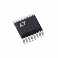
LTC2440IGN#PBF Linear Technology, LTC2440IGN#PBF Datasheet - Page 13

LTC2440IGN#PBF
Manufacturer Part Number
LTC2440IGN#PBF
Description
IC ADC DIFFER 24-BIT HS 16-SSOP
Manufacturer
Linear Technology
Datasheet
1.LTC2440CGN.pdf
(28 pages)
Specifications of LTC2440IGN#PBF
Number Of Bits
24
Sampling Rate (per Second)
3.5k
Data Interface
MICROWIRE™, Serial, SPI™
Number Of Converters
2
Power Dissipation (max)
40mW
Voltage Supply Source
Single Supply
Operating Temperature
-40°C ~ 85°C
Mounting Type
Surface Mount
Package / Case
16-SSOP (0.150", 3.90mm Width)
Lead Free Status / RoHS Status
Lead free / RoHS Compliant
Available stocks
Company
Part Number
Manufacturer
Quantity
Price
APPLICATIONS INFORMATION
Chip Select Input (CS)
The active LOW chip select, CS (Pin 11), is used to test the
conversion status and to enable the data output transfer
as described in the previous sections.
In addition, the CS signal can be used to trigger a new con-
version cycle before the entire serial data transfer has been
completed. The LTC2440 will abort any serial data transfer
in progress and start a new conversion cycle anytime a
LOW-to-HIGH transition is detected at the CS pin after the
converter has entered the data output state (i.e., after the
fi fth falling edge of SCK occurs with CS = LOW).
Serial Data Input (SDI)—Logic Level Speed Selection
The serial data input (SDI, Pin 7) is used to select the
speed/resolution of the LTC2440. A simple 2-speed control
is selectable by either driving SDI HIGH or LOW. If SDI
is grounded (pin compatible with LTC2410) the device
outputs data at 880Hz with 21 bits effective resolution. By
tying SDI HIGH, the converter enters the ultralow noise
mode (200nV
6.9Hz output rate. SDI may be driven logic HIGH or LOW
anytime during the conversion or sleep state in order to
change the speed/resolution. The conversion immediately
following the data output cycle will be valid and performed
at the newly selected output rate/resolution.
Changing SDI logic state during the data output cycle
should be avoided as speed resolution other than 6.9Hz
or 880Hz may be selected. For example, if SDI is changed
from logic 0 to logic 1 after the second rising edge of SCK,
the conversion rate will change from 880Hz to 55Hz (the
following values are listed in Table 3: OSR4 = 0, OSR3 = 0,
OSR2 = 1, OSR1 = 1 and OSR0 = 1). If SDI remains HIGH,
the conversion rate will switch to the desired 6.9Hz speed
immediately following the conversion at 55Hz. The 55Hz
rate conversion cycle will be a valid result as well as the
fi rst 6.9Hz result. On the other hand, if SDI is changed to a
1 anytime before the fi rst rising edge of SCK, the following
conversion rate will become 6.9Hz. If SDI is changed to
a 1 after the 5th rising edge of SCK, the next conversion
will remain 880Hz while all subsequent conversions will
be at 6.9Hz.
RMS
) with simultaneous 50/60Hz rejection at
Serial Data Input (SDI)—Serial Input Speed Selection
SDI may also be programmed by a serial input data
stream under control of SCK during the data output cycle,
see Figure 4. One of ten speed/resolution ranges (from
6.9Hz/200nV
Table 3. The conversion following a new selection is valid
and performed at the newly selected speed/resolution.
BUSY
The BUSY output (Pin 15) is used to monitor the state of
conversion, data output and sleep cycle. While the part is
converting, the BUSY pin is HIGH. Once the conversion is
complete, BUSY goes LOW indicating the conversion is
complete and data out is ready. The part now enters the
LOW power sleep state. BUSY remains LOW while data is
shifted out of the device. It goes HIGH at the conclusion
of the data output cycle indicating a new conversion has
begun. This rising edge may be used to fl ag the comple-
tion of the data read cycle.
SERIAL INTERFACE TIMING MODES
The LTC2440’s 2-wire, 3-wire or 4-wire interface is SPI
and MICROWIRE compatible. This interface offers several
fl exible modes of operation. These include internal/external
serial clock, 2-wire or 3-wire I/O, single cycle conversion
and autostart. The following sections describe each of
these serial interface timing modes in detail. In all these
cases, the converter can use the internal oscillator (f
LOW) or an external oscillator connected to the f
See Table 4 for a summary.
External Serial Clock, Single Cycle Operation
(SPI/MICROWIRE Compatible)
This timing mode uses an external serial clock to shift
out the conversion result and a CS signal to monitor and
control the state of the conversion cycle, see Figure 5.
The serial clock mode is selected by the EXT pin. To select
the external serial clock mode, EXT must be tied low.
The serial data output pin (SDO) is Hi-Z as long as CS is
HIGH. At any time during the conversion cycle, CS may be
pulled LOW in order to monitor the state of the converter.
While CS is pulled LOW, EOC is output to the SDO pin.
RMS
to 3.5kHz/21μV
RMS
) may be selected, see
LTC2440
13
O
2440fd
pin.
O
=


