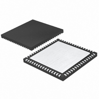
LTC2290IUP#PBF Linear Technology, LTC2290IUP#PBF Datasheet - Page 15

LTC2290IUP#PBF
Manufacturer Part Number
LTC2290IUP#PBF
Description
IC ADC DUAL 12BIT 10MSPS 64QFN
Manufacturer
Linear Technology
Datasheet
1.LTC2290CUPPBF.pdf
(24 pages)
Specifications of LTC2290IUP#PBF
Number Of Bits
12
Sampling Rate (per Second)
10M
Data Interface
Parallel
Number Of Converters
2
Power Dissipation (max)
138mW
Voltage Supply Source
Single Supply
Operating Temperature
-40°C ~ 85°C
Mounting Type
Surface Mount
Package / Case
64-WFQFN, Exposed Pad
Lead Free Status / RoHS Status
Lead free / RoHS Compliant
APPLICATIO S I FOR ATIO
The difference amplifier generates the high and low refer-
ence for the ADC. High speed switching circuits are
connected to these outputs and they must be externally
bypassed. Each output has two pins. The multiple output
pins are needed to reduce package inductance. Bypass
capacitors must be connected as shown in Figure 6. Each
ADC channel has an independent reference with its own
bypass capacitors. The two channels can be used with the
same or different input ranges.
Other voltage ranges between the pin selectable ranges
can be programmed with two external resistors as shown
in Figure 7. An external reference can be used by applying
its output directly or through a resistor divider to SENSE.
It is not recommended to drive the SENSE pin with a logic
device. The SENSE pin should be tied to the appropriate
level as close to the converter as possible. If the SENSE pin
is driven externally, it should be bypassed to ground as
close to the device as possible with a 1µF ceramic capacitor.
For the best channel matching, connect an external reference
to SENSEA and SENSEB.
Input Range
The input range can be set based on the application. The
2V input range will provide the best signal-to-noise perfor-
mance while maintaining excellent SFDR. The 1V input
range will have better SFDR performance, but the SNR will
degrade by 3.8dB.
Figure 7. 1.5V Range ADC
12k
12k
0.75V
1.5V
U
SENSE
2.2µF
1µF
U
V
CM
LTC2290
W
2290 F07
U
Driving the Clock Input
The CLK inputs can be driven directly with a CMOS or TTL
level signal. A differential clock can also be used along with
a low jitter CMOS converter before the CLK pin (Figure 8).
The noise performance of the LTC2290 can depend on the
clock signal quality as much as on the analog input. Any
noise present on the clock signal will result in additional
aperture jitter that will be RMS summed with the inherent
ADC aperture jitter.
It is recommended that CLKA and CLKB are shorted
together and driven by the same clock source. If a small
time delay is desired between when the two channels
sample the analog inputs, CLKA and CLKB can be driven
by two different signals. If this delay exceeds 1ns, the
performance of the part may degrade. CLKA and CLKB
should not be driven by asynchronous signals.
Figure 8. CLK Drive Using an LVDS or PECL to CMOS Converter
100Ω
IF LVDS USE FIN1002 OR FIN1018.
FOR PECL, USE AZ1000ELT21 OR SIMILAR
4.7µF
FERRITE
BEAD
0.1µF
CLK
SUPPLY
CLEAN
LTC2290
LTC2290
2290 F08
15
2290fa


