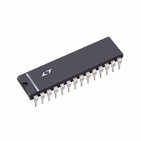
LTC1605-2CN Linear Technology, LTC1605-2CN Datasheet - Page 6

LTC1605-2CN
Manufacturer Part Number
LTC1605-2CN
Description
IC ADC 16BIT 5V SAMPLING 28DIP
Manufacturer
Linear Technology
Datasheet
1.LTC1605-1CGPBF.pdf
(20 pages)
Specifications of LTC1605-2CN
Number Of Bits
16
Sampling Rate (per Second)
100k
Data Interface
Parallel
Number Of Converters
1
Power Dissipation (max)
80mW
Voltage Supply Source
Analog and Digital
Operating Temperature
0°C ~ 70°C
Mounting Type
Through Hole
Package / Case
28-DIP (0.300", 7.62mm)
Lead Free Status / RoHS Status
Contains lead / RoHS non-compliant
V
resistor to the analog input. Full-scale input range is 0V
to 4V for the LTC1605-1 and 4V for the LTC1605-2.
AGND1 (Pin 2): Analog Ground. Tie to analog ground
plane.
REF (Pin 3): 2.5V Reference Output. Bypass with 2.2 F
tantalum capacitor. Can be driven with an external refer-
ence.
CAP (Pin 4): Reference Buffer Output. Bypass with 2.2 F
tantalum capacitor.
AGND2 (Pin 5): Analog Ground. Tie to analog ground
plane.
D15 to D8 (Pins 6 to 13): Three-State Data Outputs.
Hi-Z state when CS is high or when R/C is low.
DGND (Pin 14): Digital Ground.
D7 to D0 (Pins 15 to 22): Three-State Data Outputs.
Hi-Z state when CS is high or when R/C is low.
BYTE (Pin 23): Byte Select. With BYTE low, data will be
output with Pin 6 (D15) being the MSB and Pin 22 (D0)
LTC1605-1/LTC1605-2
FU CTIO AL BLOCK DIAGRA
PIN
6
IN
U
U
(Pin 1): Analog Input. Connect through a 200
FUNCTIONS
AGND1
AGND2
(2.5V)
DGND
CAP
REF
V
IN
U
U
*RESISTOR VALUES FOR THE LTC1605-2
6K*
4k
4k
U
REF BUF
2.5V REF
10k
OPEN*
INTERNAL
CLOCK
20k
3.75k*
16-BIT CAPACITIVE DAC
SUCCESSIVE APPROXIMATION
W
CS
C
C
SAMPLE
SAMPLE
CONTROL LOGIC
REGISTER
R/C
being the LSB. With BYTE high the upper eight bits and
the lower eight bits will be switched. The MSB is output
on Pin 15 and bit 8 is output on Pin 22. Bit 7 is output on
Pin 6 and the LSB is output on Pin 13.
R/C (Pin 24): Read/Convert Input. With CS low, a falling
edge on R/C puts the internal sample-and-hold into the
hold state and starts a conversion. With CS low, a rising
edge on R/C enables the output data bits.
CS (Pin 25): Chip Select. Internally OR’d with R/C. With
R/C low, a falling edge on CS will initiate a conversion.
With R/C high, a falling edge on CS will enable the output
data.
BUSY (Pin 26): Output Shows Converter Status. It is low
when a conversion is in progress. Data valid on the rising
edge of BUSY. CS or R/C must be high when BUSY rises
or another conversion will start without time for signal
acquisition.
V
a 0.1 F ceramic and a 10 F tantalum capacitor.
V
Pin 27.
ANA
DIG
BYTE
(Pin 27): 5V Analog Supply. Bypass to ground with
(Pin 28): 5V Digital Supply. Connect directly to
BUSY
ZEROING SWITCHES
16
+
–
COMP
OUTPUT LATCHES
1605-1/2 BD
•
•
•
D15
D0
V
V
ANA
DIG


