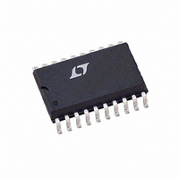
LTC1609ISW Linear Technology, LTC1609ISW Datasheet - Page 5

LTC1609ISW
Manufacturer Part Number
LTC1609ISW
Description
IC A/DCONV 16BIT SRL SAMP 20SOIC
Manufacturer
Linear Technology
Datasheet
1.LTC1609CSW.pdf
(24 pages)
Specifications of LTC1609ISW
Number Of Bits
16
Sampling Rate (per Second)
200k
Data Interface
Serial
Number Of Converters
1
Power Dissipation (max)
100mW
Voltage Supply Source
Analog and Digital
Operating Temperature
-40°C ~ 85°C
Mounting Type
Surface Mount
Package / Case
20-SOIC (0.300", 7.50mm Width)
Lead Free Status / RoHS Status
Contains lead / RoHS non-compliant
Available stocks
Company
Part Number
Manufacturer
Quantity
Price
Company:
Part Number:
LTC1609ISW
Manufacturer:
SONY
Quantity:
6 232
Part Number:
LTC1609ISW
Manufacturer:
LT/凌特
Quantity:
20 000
Company:
Part Number:
LTC1609ISW#PBF
Manufacturer:
Linear Technology
Quantity:
135
POWER REQUIREMENTS
otherwise specifications are at T
SYMBOL
V
I
P
Note 1: Absolute Maximum Ratings are those values beyond which the life
of a device may be impaired.
Note 2: All voltage values are with respect to ground with DGND, AGND1
and AGND2 wired together (unless otherwise noted).
Note 3: When these pin voltages are taken below ground or above V
V
handle input currents of greater than 100mA below ground or above V
without latch-up.
Note 4: When these pin voltages are taken below ground, they will be
clamped by internal diodes. This product can handle input currents of
90mA below ground without latchup. These pins are not clamped to V
Note 5: V
specified.
Note 6: Linearity, offset and full-scale specifications apply for a V
with respect to ground.
Note 7: Integral nonlinearity is defined as the deviation of a code from a
straight line passing through the actual end points of the transfer curve.
The deviation is measured from the center of the quantization band.
Note 8: Bipolar zero error is the offset voltage measured from – 0.5 LSB
when the output code flickers between 0000 0000 0000 0000 and 1111
1111 1111 1111. Unipolar zero error is the offset voltage measured from
0.5LSB when the output codes flickers between 0000. . .0000 and 0000. .
.0001.
DD
DD
DIS
DIG
= V
DD
DD
, they will be clamped by internal diodes. This product can
= 5V, f
PARAMETER
Positive Supply Voltage
Positive Supply Current
Power Dissipation
SAMPLE
= 200kHz, t
A
W U
r
= 25 C. (Note 5)
= t
f
= 5ns unless otherwise
The
CONDITIONS
(Notes 9, 10)
PWRD = Low
PWRD = Low
PWRD = High
indicates specifications which apply over the full operating temperature range,
IN
input
ANA
DD
DD
=
.
Note 9: Guaranteed by design, not subject to test.
Note 10: Recommended operating conditions.
Note 11: With CS low the falling R/C edge starts a conversion. If R/C
returns high at a critical point during the conversion it can create small
errors. For best results ensure that R/C returns high within 1.2 s after the
start of the conversion.
Note 12: As measured with fixed 1% resistors shown in Figures 3a and
3b. Adjustable to zero with external potentiometer.
Note 13: Full-scale error is the worst-case of –FS or +FS untrimmed
deviation from ideal first and last code transitions, divided by the transition
voltage (not divided by the full-scale range) and includes the effect of
offset error. For unipolar input ranges full-scale error is the deviation of
the last code transition from ideal divided by the transiton voltage and
includes the effect of offset error.
Note 14: All specifications in dB are referred to a full-scale 5V input.
Note 15: Full-power bandwidth is defined as full-scale input frequency at
which a signal-to-(noise + distortion) degrades to 60dB or 10 bits of
accuracy.
Note 16: Recovers to specified performance after (2 • FS) input
overvoltage.
Note 17: When data is shifted out during a conversion, with an external
data clock, complete the process within 1.2 s from the start of the
conversion (BUSY falling). This will help keep any external disturbances
from causing an error in the conversion result.
4.75
MIN
LTC1609/LTC1609A
TYP
13
65
50
LTC1609
MAX
5.25
100
20
UNITS
1609fa
5
mW
mA
W
V


