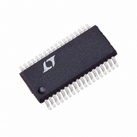
LTC1411CG#PBF Linear Technology, LTC1411CG#PBF Datasheet

LTC1411CG#PBF
Specifications of LTC1411CG#PBF
Related parts for LTC1411CG#PBF
LTC1411CG#PBF Summary of contents
Page 1
... Internal or External Reference Sleep (1 A) and Nap (2mA) Shutdown Modes 36-Pin SSOP Package U APPLICATIO S Telecommunications High Speed Data Acquisition Digital Signal Processing Multiplexed Data Acquisition Systems Spectrum Analysis Imaging Systems , LTC and LT are registered trademarks of Linear Technology Corporation. W BLOCK DIAGRA + – ...
Page 2
LTC1411 ABSOLUTE AXI U RATI GS AVP = DVP = (Notes Supply Voltage (V ) ................................................. 6V DD Analog Input Voltage (Note 3) ... – 0. Digital Input ...
Page 3
ALOG I PUT (Note 5) A SYMBOL PARAMETER V Analog Input Range (Note 9) IN Common Mode Input Range C Analog Input Capacitance IN t Sample-and-Hold Acquisition Time ACQ t Sample-and-Hold Aperture Delay ...
Page 4
LTC1411 CHARACTERISTICS range, otherwise specifications are (Notes 5) (See Figures 11a, 11b) A SYMBOL PARAMETER f Maximum Sampling Frequency SAMPLE(MAX) t Conversion Time CONV t Acquisition Time ACQ t SLP to ...
Page 5
W U TYPICAL PERFOR A CE CHARACTERISTICS Spurious Free Dynamic Range vs Input Frequency 0 –10 –20 –30 –40 –50 –60 –70 –80 –90 –100 –110 10 100 1000 10000 INPUT FREQUENCY (kHz) 1411 G04 Differential Nonlinearity vs Output Code ...
Page 6
LTC1411 W U TYPICAL PERFOR A CE CHARACTERISTICS 4096 Points FFT Plot (1MHz) 0 SINAD = 75dB SFDR = 81dB – 2.5MHz SAMPLE f = 1MHz IN –40 –60 –80 –100 –120 –140 250 500 0 FREQUENCY (kHz) ...
Page 7
CTIO S DVP (Pin 30): 5V Digital Power Supply Pin. Bypass to OGND with tantalum capacitor. DGND (Pin 31): Digital Ground. CONVST (Pin 32): Conversion Start Signal. This active low signal starts ...
Page 8
LTC1411 TEST CIRCUITS Load Circuits for Access Timing (A) Hi AND (B) Hi AND APPLICATIO S I ...
Page 9
U U APPLICATIO S I FOR ATIO 0 SINAD = 78.8dB SFDR = 95dB –20 f SAMPLE f = 100kHz IN –40 –60 –80 –100 –120 –140 0 250 500 750 INPUT FREQUENCY (kHz) Figure 2a. LTC1411 Nonaveraged, 4096 Point ...
Page 10
... DC accuracy and settling time are most critical. The following list is a summary of the op amps that are suitable for driving the LTC1411. More detailed information is available in the Linear Technology Databooks and on the LinearView ® LT 1227: 140MHz Video Current Feedback Amplifier ...
Page 11
U U APPLICATIO S I FOR ATIO LT6203: Dual 100MHz, Low Noise, Low Power Op Amp. Specified at 3V, 5V and 5V supplies. 1.9nV/ Hz noise voltage. Programmable Input Range The LTC1411 has two logic input pins (PGA0 and PGA1) ...
Page 12
LTC1411 U U APPLICATIO S I FOR ATIO Figure 7 shows a typical reference, the LT1019A-2.5 connected to the LTC1411. This will provide an improved drift (equal to the maximum 5ppm the LT1019A-2.5). INPUT RANGE: 0.7V TO 4.3V ...
Page 13
U U APPLICATIO S I FOR ATIO An analog ground plane separate from the logic system ground should be established under and around the ADC. AGND1 (Pins 7 to 9), AVM (Pin 11), DGND (Pin 31) and OGND ...
Page 14
LTC1411 U U APPLICATIO S I FOR ATIO (SAMPLE CONVST t 3 BUSY DATA (N – 1) DATA DB13 TO DB0 Figure 11a. CONVST Starts a Conversion with a Short Active Low Pulse t 5 (SAMPLE N) ...
Page 15
... FLASH SHALL NOT EXCEED .254mm (.010") PER SIDE Information furnished by Linear Technology Corporation is believed to be accurate and reliable. However, no responsibility is assumed for its use. Linear Technology Corporation makes no represen- tation that the interconnection of its circuits as described herein will not infringe on existing patent rights. ...
Page 16
... Single 5V Supply www.linear.com 30 DVP OGND 28 D13 12 14 • 14-BIT • OUTPUT • DATA OUTPUT DRIVERS D0 25 BUSY 27 OTR 26 DGND CONVST 32 31 1411 TA03 2.5MHz CONVERT INPUT INPUT RANGE SELECTION LT/TP 0902 2K • PRINTED IN USA LINEAR TECHNOLOGY CORPORATION 2001 1411f ...


