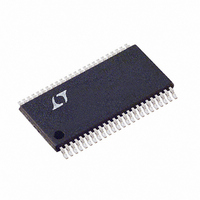
LTC1744IFW#PBF Linear Technology, LTC1744IFW#PBF Datasheet - Page 14

LTC1744IFW#PBF
Manufacturer Part Number
LTC1744IFW#PBF
Description
IC ADC 14BIT 50MSPS 48-TSSOP
Manufacturer
Linear Technology
Datasheet
1.LTC1744CFWPBF.pdf
(24 pages)
Specifications of LTC1744IFW#PBF
Number Of Bits
14
Sampling Rate (per Second)
50M
Data Interface
Parallel
Number Of Converters
1
Power Dissipation (max)
1.5W
Voltage Supply Source
Single Supply
Operating Temperature
-40°C ~ 85°C
Mounting Type
Surface Mount
Package / Case
48-TFSOP (0.240", 6.10mm Width)
Lead Free Status / RoHS Status
Lead free / RoHS Compliant
Available stocks
Company
Part Number
Manufacturer
Quantity
Price
LTC1744
APPLICATIO S I FOR ATIO
Input Drive Circuits
Figure 3 shows the LTC1744 being driven by an RF
transformer with a center tapped secondary. The second-
ary center tap is DC biased with V
signal at its optimum DC level. Figure 3 shows a 1:1 turns
ratio transformer. Other turns ratios can be used if the
source impedence seen by the ADC does not exceed 100
for each ADC input. A disadvantage of using a transformer
is the loss of low frequency response. Most small RF
transformers have poor performance at frequencies be-
low 1MHz.
Figure 4a demonstrates the use of operational amplifiers
to convert a single ended input signal into a differential
input signal. The advantage of this method is that it
provides low frequency input response; however, the
limited gain bandwidth of most op amps will limit the
SFDR at high input frequencies.
Figure 4b shows the LT6600, a low noise differential
amplifier and lowpass filter, used as an input driver. The
LT6600 provides two functions: it serves as a 4th order
lowpass filter and as a single-ended to differential con-
verter. Additionally it can be programmed with one exter-
nal resistor to provide a gain from 1 to 4. Three versions
of this device are available having lowpass filter band-
widths of 2.5MHz, 10MHz or 20MHz.
The 37
inputs serve two purposes: isolating the drive circuitry
from the sample-and-hold charging glitches and limiting
the wideband noise at the converter input. For input
14
ANALOG
INPUT
resistors and 18pF capacitors on the analog
0.1 F
Figure 3. Single-Ended to Differential
Conversion Using a Transformer
100
U
1:1
U
100
37
37
CM
, setting the ADC input
W
18pF
4.7 F
18pF
18pF
V
A
A
CM
IN
IN
+
–
LTC1744
U
1744 F03
frequencies higher than 40MHz, the capacitors may need
to be decreased to prevent excessive signal loss.
Reference Operation
Figure 5 shows the LTC1744 reference circuitry consisting
of a 2.5V bandgap reference, a difference amplifier and
switching and control circuit. The internal voltage refer-
ence can be configured for two pin selectable input ranges
of 2V( 1V differential) or 3.2V( 1.6V differential). Tying
the SENSE pin to ground selects the 2V range; tying the
SENSE pin to V
The 2.5V bandgap reference serves two functions: its
output provides a DC bias point for setting the common
mode voltage of any external input circuitry; additionally,
the reference is used with a difference amplifier to gener-
ate the differential reference levels needed by the internal
ADC circuitry.
2.5V 1/2 RANGE
SINGLE-ENDED
V
Figure 4b. Using the LT6600 as a Differential Driver
IN
INPUT
Figure 4a. Differential Drive with Op Amps
0.01 F
402
402
R
R
IN
IN
DD
100
500
1
2
7
8
selects the 3.2V range.
–
V
V
+
LT6600-20
OCM
MID
5V
3
6
–
–
+
+
+
–
1/2 LT1810
1/2 LT1810
4
5
5V
GAIN = 402 /R
MAXIMUM GAIN = 4
500
0.1 F
49.9
49.9
37
37
18pF
IN
1 F
V
A
A
CM
IN
IN
+
–
18pF
LTC1744
4.7 F
18pF
18pF
V
A
A
CM
IN
IN
1744 F04b
+
–
LTC1744
1744 F04a
1744f


