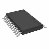
AD7366BRUZ-5 Analog Devices Inc, AD7366BRUZ-5 Datasheet - Page 20

AD7366BRUZ-5
Manufacturer Part Number
AD7366BRUZ-5
Description
IC ADC 12BIT DUAL 500KSPS 24-TSS
Manufacturer
Analog Devices Inc
Datasheet
1.AD7367BRUZ-5.pdf
(28 pages)
Specifications of AD7366BRUZ-5
Data Interface
DSP, MICROWIRE™, QSPI™, Serial, SPI™
Design Resources
Driving the AD7366/7 Bipolar SAR ADC in Low-Distortion DC-Coupled Appls (CN0042)
Number Of Bits
12
Sampling Rate (per Second)
500k
Number Of Converters
2
Power Dissipation (max)
88.8mW
Voltage Supply Source
Analog and Digital, Dual ±
Operating Temperature
-40°C ~ 85°C
Mounting Type
Surface Mount
Package / Case
24-TSSOP (0.173", 4.40mm Width)
Resolution (bits)
12bit
Input Channel Type
Single Ended
Supply Voltage Range - Analogue
4.75V To 5.25V, ± 11.5V To ± 16.5V
Supply Voltage Range - Digital
2.7V To 5.25V,
Sampling Rate
1MSPS
Rohs Compliant
Yes
Lead Free Status / RoHS Status
Lead free / RoHS Compliant
For Use With
EVAL-AD7366CBZ - BOARD EVALUATION FOR AD7366
Lead Free Status / RoHS Status
Lead free / RoHS Compliant, Lead free / RoHS Compliant
Available stocks
Company
Part Number
Manufacturer
Quantity
Price
Company:
Part Number:
AD7366BRUZ-5
Manufacturer:
ADI
Quantity:
1 000
Part Number:
AD7366BRUZ-5
Manufacturer:
ADI/亚德诺
Quantity:
20 000
Company:
Part Number:
AD7366BRUZ-5-RL7
Manufacturer:
ADI
Quantity:
1 000
AD7366-5/AD7367-5
MODES OF OPERATION
The mode of operation for the AD7366-5/AD7367-5 is selected
by the (logic) state of the CNVST signal at the end of a conver-
sion. There are two possible modes of operation: normal mode
and shutdown mode. These modes of operation are designed to
provide flexible power management options, which can be
chosen to optimize the power dissipation/throughput rate
ratio for differing application requirements.
NORMAL MODE
Normal mode is intended for applications needing fast
throughput rates because the user does not have to worry
about any power-up times (with the AD7366-5/AD7367-5
remaining fully powered at all times). Figure 22 shows the
normal mode of operation for the AD7366-5, while Figure 23
illustrates normal mode for the AD7367-5.
The conversion is initiated on the falling edge of CNVST as
described in the
the part remains fully powered up at all times,
at a logic high state prior to the BUSY signal going low. If
CNVST is at a logic low state when the BUSY signal goes low,
the analog circuitry powers down and the part ceases converting.
Circuit Information
CNVST
CNVST
BUSY
BUSY
SCLK
SCLK
CS
CS
t
t
2
2
section. To ensure that
SERIAL READ OPERATION
t
SERIAL READ OPERATION
t
1
1
CNVST must be
Figure 22. Normal Mode Operation for the AD7366-5
Figure 23. Normal Mode Operation for the AD7367-5
t
t
CONVERT
CONVERT
Rev. A | Page 20 of 28
1
1
t
t
3
3
The BUSY signal remains high for the duration of the conversion.
The CS pin must be brought low to bring the data bus out of
three-state; subsequently 12 SCLK cycles are required to read
the conversion result from the AD7366-5, while 14 SCLK cycles
are required to read from the AD7367-5. The D
to three-state only when CS is brought high. If CS is left low for
a further 12 SCLK cycles for the AD7366-5 or 14 SCLK cycles
for the AD7367-5, the result from the other on-chip ADC is
also accessed on the same D
Figure 28
After 24 SCLK cycles have elapsed for the AD7366-5 and 28 SCLK
cycles have elapsed for the AD7367-5, the D
three-state when CS is brought high (not on the 24
falling edge). If CS is brought high prior to this, the D
returns to three-state at that point. Thus, CS must be brought
high once the read is completed because the bus does not
automatically return to three-state upon completion of the
dual result read.
Once a data transfer is complete and D
returned to three-state, another conversion can be initiated after
the quiet time, t
(see the
QUIET
t
t
QUIET
QUIET
Serial Interface
, has elapsed by bringing CNVST low again.
14
12
OUT
line, as shown in
section).
OUT
A and D
OUT
OUT
line returns to
Figure 27
th
OUT
or 28
lines return
B have
OUT
th
line
SCLK
and


