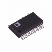
AD9201ARS Analog Devices Inc, AD9201ARS Datasheet - Page 4

AD9201ARS
Manufacturer Part Number
AD9201ARS
Description
IC ADC CMOS 10BIT DUAL 28-SSOP
Manufacturer
Analog Devices Inc
Specifications of AD9201ARS
Mounting Type
Surface Mount
Rohs Status
RoHS non-compliant
Number Of Bits
10
Sampling Rate (per Second)
20M
Data Interface
Parallel
Number Of Converters
2
Power Dissipation (max)
245mW
Voltage Supply Source
Analog and Digital
Operating Temperature
-40°C ~ 85°C
Package / Case
28-SSOP (0.200", 5.30mm Width)
Input Channels Per Adc
2
No. Of Channels
2
Peak Reflow Compatible (260 C)
No
Inl ±
2.5LSB
Sample Rate
20MSPS
No. Of Bits
10 Bit
Leaded Process Compatible
No
Dnl±
1LSB
Number Of Elements
2
Resolution
10Bit
Architecture
Pipelined
Input Polarity
Unipolar
Input Type
Voltage
Rated Input Volt
1.5V
Differential Input
Yes
Power Supply Requirement
Analog and Digital
Single Supply Voltage (typ)
3V
Single Supply Voltage (min)
2.7V
Single Supply Voltage (max)
5.5V
Dual Supply Voltage (typ)
Not RequiredV
Dual Supply Voltage (min)
Not RequiredV
Dual Supply Voltage (max)
Not RequiredV
Differential Linearity Error
±1LSB
Integral Nonlinearity Error
±2.5LSB
Operating Temp Range
-40C to 85C
Operating Temperature Classification
Industrial
Mounting
Surface Mount
Pin Count
28
Package Type
SSOP
Lead Free Status / Rohs Status
Not Compliant
Available stocks
Company
Part Number
Manufacturer
Quantity
Price
Part Number:
AD9201ARS
Manufacturer:
ADI/亚德诺
Quantity:
20 000
Part Number:
AD9201ARSZ
Manufacturer:
ADI/亚德诺
Quantity:
20 000
Company:
Part Number:
AD9201ARSZ-REEL
Manufacturer:
SIEMENS
Quantity:
3
CAUTION
ESD (electrostatic discharge) sensitive device. Electrostatic charges as high as 4000 V readily
accumulate on the human body and test equipment and can discharge without detection.
Although the AD9201 features proprietary ESD protection circuitry, permanent damage may
occur on devices subjected to high energy electrostatic discharges. Therefore, proper ESD
precautions are recommended to avoid performance degradation or loss of functionality.
AD9201
ABSOLUTE MAXIMUM RATINGS*
Parameter
AVDD
DVDD
AVSS
AVDD
CLK
Digital Outputs
AINA, AINB
VREF
REFSENSE
REFT, REFB
Junction Temperature
Storage Temperature
Lead Temperature
*Stresses above those listed under Absolute Maximum Ratings may cause perma-
Model
AD9201ARS
AD9201-EVAL
*RS = Shrink Small Outline.
nent damage to the device. This is a stress rating only; functional operation of the
device at these or any other conditions above those indicated in the operational
sections of this specification is not implied. Exposure to absolute maximum ratings
for extended periods may effect device reliability.
10 sec
(MSB) D9
(LSB) D0
SELECT
CLOCK
DVDD
DVSS
Temperature
Range
–40 C to +85 C
PIN CONFIGURATION
D1
D2
D3
D4
D5
D6
D7
D8
With
Respect
to
AVSS
DVSS
DVSS
DVDD
AVSS
DVSS
AVSS
AVSS
AVSS
AVSS
ORDERING GUIDE
(Not to Scale)
TOP VIEW
AD9201
Min
–0.3
–0.3
–0.3
–6.5
–0.3
–0.3
–1.0
–0.3
–0.3
–0.3
–65
Package
Description
28-Lead SSOP
Evaluation Board
CHIP-SELECT
INA-Q
INB-Q
REFT-Q
REFB-Q
AVDD
VREF
REFSENSE
AVSS
REFB-I
REFT-I
INB-I
INA-I
SLEEP
Max
+6.5
+6.5
+0.3
+6.5
AVDD + 0.3
DVDD + 0.3
AVDD + 0.3
AVDD + 0.3
AVDD + 0.3
AVDD + 0.3
+150
+150
+300
Package
Options*
RS-28
Units
V
V
V
V
V
V
V
V
V
V
C
C
C
–4–
P
No.
1
2
3
4
5
6
7
8
9
10
11
12
13
14
15
16
17
18
19
20
21
22
23
24
25
26
27
28
DEFINITIONS OF SPECIFICATIONS
INTEGRAL NONLINEARITY (INL)
Integral nonlinearity refers to the deviation of each individual
code from a line drawn from “zero” through “full scale.” The
point used as “zero” occurs 1/2 LSB before the first code tran-
sition. “Full scale” is defined as a level 1 1/2 LSBs beyond the
last code transition. The deviation is measured from the center
of each particular code to the true straight line.
DIFFERENTIAL NONLINEARITY (DNL, NO MISSING
CODES)
An ideal ADC exhibits code transitions that are exactly 1 LSB
apart. DNL is the deviation from this ideal value. It is often
specified in terms of the resolution for which no missing codes
(NMC) are guaranteed.
in
Name
DVSS
DVDD
D0
D1
D2
D3
D4
D5
D6
D7
D8
D9
SELECT
CLOCK
SLEEP
INA-I
INB-I
REFT-I
REFB-I
AVSS
REFSENSE
VREF
AVDD
REFB-Q
REFT-Q
INB-Q
INA-Q
CHIP-SELECT Hi-High Impedance, Lo-Normal Operation
PIN FUNCTION DESCRIPTIONS
Description
Digital Ground
Digital Supply
Bit 0 (LSB)
Bit 1
Bit 2
Bit 3
Bit 4
Bit 5
Bit 6
Bit 7
Bit 8
Bit 9 (MSB)
Hi I Channel Out, Lo Q Channel Out
Clock
Hi Power Down, Lo Normal Operation
I Channel, A Input
I Channel, B Input
Top Reference Decoupling, I Channel
Bottom Reference Decoupling, I Channel
Analog Ground
Reference Select
Internal Reference Output
Analog Supply
Bottom Reference Decoupling, Q Channel
Top Reference Decoupling, Q Channel
Q Channel, B Input
Q Channel, A Input
WARNING!
ESD SENSITIVE DEVICE
REV. D


