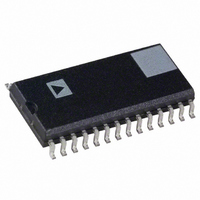
AD9220AR Analog Devices Inc, AD9220AR Datasheet - Page 24

AD9220AR
Manufacturer Part Number
AD9220AR
Description
IC ADC 12BIT 10MSPS 28-SOIC
Manufacturer
Analog Devices Inc
Datasheet
1.AD9220ARSZ-REEL.pdf
(32 pages)
Specifications of AD9220AR
Mounting Type
Surface Mount
Rohs Status
RoHS non-compliant
Number Of Bits
12
Sampling Rate (per Second)
10M
Data Interface
Parallel
Number Of Converters
7
Power Dissipation (max)
310mW
Voltage Supply Source
Single Supply
Operating Temperature
-40°C ~ 85°C
Package / Case
28-SOIC (0.300", 7.50mm Width)
Power Dissipation Pd
310mW
Input Channels Per Adc
1
No. Of Channels
1
Peak Reflow Compatible (260 C)
No
Sample Rate
10MSPS
Supply Voltage Max
5V
No. Of Bits
12 Bit
For Use With
AD9220-EB - BOARD EVAL FOR AD9220
Lead Free Status / RoHS Status
Contains lead / RoHS non-compliant
Available stocks
Company
Part Number
Manufacturer
Quantity
Price
Part Number:
AD9220AR
Manufacturer:
ADI/亚德诺
Quantity:
20 000
Company:
Part Number:
AD9220ARS
Manufacturer:
AD
Quantity:
5 510
Part Number:
AD9220ARS
Manufacturer:
ADI/亚德诺
Quantity:
20 000
Part Number:
AD9220ARSZ
Manufacturer:
ADI/亚德诺
Quantity:
20 000
Part Number:
AD9220ARSZ-REEL
Manufacturer:
ADI/亚德诺
Quantity:
20 000
Part Number:
AD9220ARSZRL
Manufacturer:
ADI/亚德诺
Quantity:
20 000
AD9221/AD9223/AD9220
The offset calibration circuitry consists of a DAC, U5 and
the buffer amplifier, U4. The DAC is configured for a bipolar
adjustment span of ± 64 LSB with a 1/2 LSB resolution span
with respect to the AD9221/AD9223/AD9220. Note that both
current outputs of U5 were configured to provide a bipolar
adjustment span. Also, RC is used to decouple the output of
both DACs, U3 and U5, from their respective op amps.
The calibration procedure consists of a two step process. First,
the bipolar offset is calibrated by selecting CH2, the 2.5 V sys-
tem reference, of the analog multiplexer and preloading the DAC,
U5, with a midscale code of 1000 0000. If possible, several
readings of the A/D should be taken and averaged to determine
the required digital offset adjustment code, U5. This averaged
offset code requires an extra bit of resolution since 1 LSB of U5
equates to 1/2 LSB of the AD9221/AD9223/AD9220. The
required offset correction code to U5 can then be determined.
Second, the system gain is calibrated by selecting CH2, a 1.25 V
2.50V
1.25V
CH1
CH2
CH3
CH4
CH5
CH6
CH7
CH8
ADG608
1.25k
U6
0.1 F
U2B
2.5k
OUT
Figure 35. Typical Multichannel Data Acquisition System
0.1 F
0.1 F
2.5k
10 F
U4
2.5k
2.5k
2.5k
VREF(+)
VREF(–)
REF43
U1
162
2.5k
2.5k
DAC08
U3
2.5k
–24–
VREF(+)
VREF(–)
IOUT
IOUT
0.1 F
input that corresponds to –FS of the A/D. Before the value is
read, U4 should be preloaded with a code of 00 (Hex). Several
readings can also be taken and averaged to determine the digital
gain adjustment code to U2A. In this case, 1 LSB of the A/D
corresponds to 1 LSB of U4.
Due to the AD9221/AD9223/AD9220’s excellent INL perfor-
mance, a two-point calibration procedure (i.e., –FS to midscale)
instead of an endpoint calibration procedure was chosen. Also,
since the bipolar offset is insensitive to any gain adjustment (due
to the differential SHA of the A/D), an iterative calibration
process is not required. The temperature stability of the circuit
is enhanced by selecting a dual precision op amp for U2 (e.g.,
OP293) and low temperature drift, thin film resistors. Note that
this application circuit was not built at the release of this data
sheet. Please consult Analog Devices for application assistance
or comments.
1.1k
DAC08
39
39
U5
R
100
C
2
U2A
39
IOUT
IOUT
R
100
C
1.25V
39mV
+5V
R
100
C
SENSE
VREF
VINA
VINB
AD9221/
AD9223/
AD9220
BIT 1 – BIT 12
OTR
REV. E


