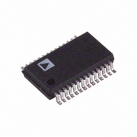
AD9225ARS Analog Devices Inc, AD9225ARS Datasheet - Page 15

AD9225ARS
Manufacturer Part Number
AD9225ARS
Description
IC ADC 12BIT 25MSPS 28-SSOP
Manufacturer
Analog Devices Inc
Datasheet
1.AD9225ARZ.pdf
(25 pages)
Specifications of AD9225ARS
Mounting Type
Surface Mount
Package / Case
28-SSOP (0.200", 5.30mm Width)
Rohs Status
RoHS non-compliant
Number Of Bits
12
Sampling Rate (per Second)
25M
Data Interface
Parallel
Number Of Converters
7
Power Dissipation (max)
373mW
Voltage Supply Source
Single Supply
Operating Temperature
-40°C ~ 85°C
Peak Reflow Compatible (260 C)
No
No. Of Bits
12 Bit
Leaded Process Compatible
No
No. Of Channels
2
Interface Type
Parallel
For Use With
AD9225-EB - BOARD EVAL FOR AD9225
Lead Free Status / RoHS Status
Contains lead / RoHS non-compliant
Available stocks
Company
Part Number
Manufacturer
Quantity
Price
Company:
Part Number:
AD9225ARS
Manufacturer:
ADI
Quantity:
288
Part Number:
AD9225ARS
Manufacturer:
ADI/亚德诺
Quantity:
20 000
Part Number:
AD9225ARSRL
Manufacturer:
ADI/亚德诺
Quantity:
20 000
Company:
Part Number:
AD9225ARSZ
Manufacturer:
ADI
Quantity:
1 000
Part Number:
AD9225ARSZ
Manufacturer:
ADI/亚德诺
Quantity:
20 000
Company:
Part Number:
AD9225ARSZRL
Manufacturer:
ADI
Quantity:
1 000
Rev. C
Figure 13 shows the schematic of the suggested transformer circuit.
The circuit uses a minicircuits RF transformer, model #T4-1T,
which has an impedance ratio of 4 (turns ratio of 2). The sche-
matic assumes that the signal source has a 50 W source impedance.
The 1:4 impedance ratio requires the 200 W secondary termination
for optimum power transfer and VSWR. The center tap of the
transformer provides a convenient means of level-shifting the input
signal to a desired common-mode voltage.
The configuration in Figure 13 was used to gather the differential
data on the Specifications tables.
Transformers with other turns ratios may also be selected to opti-
mize the performance of a given application. For example, a given
input signal source or amplifier may realize an improvement in
distortion performance at reduced output power levels and signal
swings. For example, selecting a transformer with a higher imped-
ance ratio (e.g., Minicircuits T16-6T with a 1:16 impedance ratio)
effectively steps up the signal level further reducing the driving
requirements of the signal source.
Referring to Figure 13, a series resistors, R
C
transformer. The value of 33 W was selected to specifically opti-
mize both the THD and SNR performance of the ADC. R
C
The AD9225 can be easily configured for either a 2 V p-p input
span or a 4.0 V p-p input span by setting the internal reference (see
Table II). Other input spans can be realized with two external gain
setting resistors as shown in Figure 19. Figures 14 and 15 demon-
strate how both spans of the AD9225 achieve the high degree of
linearity and SFDR over a wide range of amplitudes required by
the most demanding communication applications.
Figures 14 and 15 demonstrate the flexibility of common-mode
voltage (transformer center tap) with respect to THD.
S
S
, were inserted between the AD9225 and the secondary of the
help provide a low-pass filter to block high frequency noise.
49.9
Figure 13. Transformer Coupled Input
MINICIRCUITS
T4-1T
200
33
33
R
R
S
S
0.1 F
C
S
S
, and shunt capacitor,
VINA
VINB
CML
AD9225
S
and
–15–
–100.0
–110.0
–119.7
–10.0
–20.0
–30.0
–40.0
–50.0
–60.0
–70.0
–80.0
–90.0
Figure 16. Single-Tone Frequency Domain Plot
Common-Mode Voltage = 2.5 V (A
Differential)
0.0
–76
–78
–80
–82
–84
–86
–76
–78
–80
–82
–84
–86
Figure 14. Common-Mode Voltage vs. THD
(A
Figure 15. Common-Mode Voltage vs. THD
(A
0.5
IN
IN
0
= 2 V Differential)
= 4 V Differential)
2.0E+6
1.0
1
FUND
f
1.5
f
IN
f
IN
IN
4.0E+6
COMMON-MODE VOLTAGE (V)
COMMON-MODE VOLTAGE (V)
= 2.5MHz
= 2.5MHz
= 10MHz
f
IN
= 10MHz
2.0
2ND
2
6.0E+6
2.5
3RD
8.0E+6
3
3.0
10.0E+6
3.5
f
f
IN
IN
S
4TH
= 25MHz
= 2.5MHz
= 4 V
AD9225
4
4.0
12.5E+6
4.5
5


