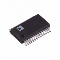
AD9226ARSZ Analog Devices Inc, AD9226ARSZ Datasheet - Page 19

AD9226ARSZ
Manufacturer Part Number
AD9226ARSZ
Description
IC ADC 12BIT 65MSPS 28-SSOP
Manufacturer
Analog Devices Inc
Datasheet
1.AD9226ASTZ.pdf
(28 pages)
Specifications of AD9226ARSZ
Data Interface
Parallel
Number Of Bits
12
Sampling Rate (per Second)
65M
Number Of Converters
3
Power Dissipation (max)
475mW
Voltage Supply Source
Single Supply
Operating Temperature
-40°C ~ 85°C
Mounting Type
Surface Mount
Package / Case
28-SSOP (0.200", 5.30mm Width)
Resolution (bits)
12bit
Sampling Rate
65MSPS
Input Channel Type
Differential, Single Ended
Supply Voltage Range - Analog
4.75V To 5.25V
Supply Current
86mA
Lead Free Status / RoHS Status
Lead free / RoHS Compliant
For Use With
AD9226-EB - BOARD EVAL FOR AD9226-SSOP
Lead Free Status / RoHS Status
Lead free / RoHS Compliant, Lead free / RoHS Compliant
Available stocks
Company
Part Number
Manufacturer
Quantity
Price
Part Number:
AD9226ARSZ
Manufacturer:
ADI/亚德诺
Quantity:
20 000
Part Number:
AD9226ARSZRL
Manufacturer:
ADI/亚德诺
Quantity:
20 000
MODE CONTROLS
Clock Stabilizer
The clock stabilizer is a circuit that desensitizes the ADC from
clock duty cycle variations. The AD9226 eases system clock
constraints by incorporating a circuit that restores the internal duty
cycle to 50%, independent of the input duty cycle. Low jitter on
the rising edge (sampling edge) of the clock is preserved while
the noncritical falling edge is generated on-chip.
It may be desirable to disable the clock stabilizer, and may be
necessary when the clock frequency speed is varied or completely
stopped. Once the clock frequency is changed, over 100 clock
cycles may be required for the clock stabilizer to settle to a dif-
ferent speed. When the stabilizer is disabled, the internal switching
will be directly affected by the clock state. If the external clock is
high, the SHA will be in hold. If the clock pulse is low, the SHA
will be in track. TPC 16 shows the benefits of using the clock
stabilizer. See Tables I and III.
Data Format Select (DFS)
The AD9226 may be set for binary or two’s complement data
output formats. See Tables I and II.
SSOP Package
The SSOP mode control (Pin 22) has two functions. It enables/
disables the clock stabilizer and determines the output data format.
The exact functions of the mode pin are outlined in Table I.
Mode
DNC
AVDD
GND
10 kΩ
Resistor
LQFP Package
Pin 35 of the LQFP package determines the output data format
(DFS). If it is connected to AVSS, the output word will be straight
binary. If it is connected to AVDD, the output data format will
be two’s complement. See Table II.
Pin 43 of the LQFP package controls the clock stabilizer function
of the AD9226. If the pin is connected to AVSS, both clock
edges will be used in the conversion architecture. When Pin 43
is connected to AVDD, the internal duty cycle will be determined
by the clock stabilizer function within the ADC. See Table III.
DFS Function
Straight Binary
Two’s Complement
Clock Restore Function
Clock Stabilizer Enabled
Clock Stabilizer Disabled
DFS
Binary
Binary
Two’s Complement
Two’s Complement
To GND
Table III. Clock Stabilizer Pin
Table I. Mode Select (SSOP)
Table II. DFS Pin Controls
Clock Duty Cycle Shaping
Clock Stabilizer Disabled
Clock Stabilizer Enabled
Clock Stabilizer Enabled
Clock Stabilizer Disabled
Pin 35 Connection
AVSS
AVDD
Pin 43 Connection
AVDD
AVSS
DIGITAL INPUTS AND OUTPUTS
Digital Outputs
Table IV details the relationship among the ADC input, OTR, and
straight binary output.
Input (V)
VINA–VINB < – VREF
VINA–VINB = – VREF
VINA–VINB = 0
VINA–VINB = + VREF – 1 LSB 1111 1111 1111
VINA–VINB ≥ + VREF
Out of Range (OTR)
An out-of-range condition exists when the analog input voltage
is beyond the input range of the converter. OTR is a digital
output that is updated along with the data output corresponding
to the particular sampled analog input voltage. Hence, OTR has
the same pipeline delay (latency) as the digital data. It is LOW
when the analog input voltage is within the analog input range.
It is HIGH when the analog input voltage exceeds the input
range as shown in Figure 14. OTR will remain HIGH until the
analog input returns within the input range and another conversion
is completed. By logical ANDing OTR with the MSB and its
complement, overrange high or underrange low conditions can be
detected. Table V is a truth table for the over/underrange
circuit in Figure 15, which uses NAND gates. Systems requiring
programmable gain conditioning of the AD9226 input signal
can immediately detect an out-of-range condition, thus elimi-
nating gain selection iterations. Also, OTR can be used for
digital offset and gain calibration.
OTR DATA OUTPUTS
0
0
1
1
0
0
OTR
0
0
1
1
MSB
MSB
OTR
1111 1111 1111
1111 1111 1111
1111 1111 1110
0000 0000 0001
0000 0000 0000
0000 0000 0000
Condition (V)
Table V. Out-of-Range Truth Table
Table IV. Output Data Format
MSB
0
1
0
1
OTR
–FS – 1/2 LSB
Binary
Output Mode
0000 0000 0000
0000 0000 0000
1000 0000 0000
1111 1111 1111
–FS +1/2 LSB
–FS
Analog Input Is
In Range
In Range
Underrange
Overrange
Two’s
Complement
Mode
1000 0000 0000
1000 0000 0000
0000 0000 0000
0111 1111 1111
0111 1111 1111
+FS – 1 1/2 LSB
OVER = 1
UNDER = 1
AD9226
+FS – 1/2 LSB
+FS
OTR
1
0
0
0
1


