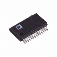
AD9226ARS Analog Devices Inc, AD9226ARS Datasheet - Page 17

AD9226ARS
Manufacturer Part Number
AD9226ARS
Description
IC ADC 12BIT 65MSPS 28-SSOP
Manufacturer
Analog Devices Inc
Datasheet
1.AD9226ASTZ.pdf
(28 pages)
Specifications of AD9226ARS
Rohs Status
RoHS non-compliant
Number Of Bits
12
Sampling Rate (per Second)
65M
Data Interface
Parallel
Number Of Converters
3
Power Dissipation (max)
475mW
Voltage Supply Source
Single Supply
Operating Temperature
-40°C ~ 85°C
Mounting Type
Surface Mount
Package / Case
28-SSOP (0.200", 5.30mm Width)
For Use With
AD9226-EB - BOARD EVAL FOR AD9226-SSOP
Available stocks
Company
Part Number
Manufacturer
Quantity
Price
Part Number:
AD9226ARS
Manufacturer:
ADI/亚德诺
Quantity:
20 000
Part Number:
AD9226ARSZ
Manufacturer:
ADI/亚德诺
Quantity:
20 000
Part Number:
AD9226ARSZRL
Manufacturer:
ADI/亚德诺
Quantity:
20 000
The low-impedance VREF output can be used to provide dc
bias levels to the fixed VINB pin and the signal on VINA. Fig-
ure 9b shows the VREF configured for 2.0 V, thus the input
range of the ADC is 1.0 V to 3.0 V. Other input ranges could
be selected by changing VREF.
When the inputs are biased from the reference (Figure 9b),
there may be a slight degeneration of dynamic performance. A
midsupply output level is available at the CM LEVEL pin of the
LQFP package.
V
IN
V
+1V
–1V
0V
IN
0.1 F
–84
–83
–82
–81
–80
–79
–78
–77
–76
+5V
–5V
0
10 F
0.5
10 F
0.1 F
3.5
2.5
1.5
C1
C2
10 F
0.1 F
10 F
1.0
V
R
R
1.5
1k
1k
R
R
0.1 F
V
S
S
15pF
R
R
R
R
2.0
S
S
10 F
15pF
10 F
Volts
2.5
VINA
VINB
VINA
VINB
3.0
AD9226
AD9226
VREF
VREF
3.5
CAPT
CAPB
0.1 F
0.1 F
CAPT
CAPB
4.0
0.1 F
0.1 F
4.5
0.1 F
0.1 F
0.1 F
5.0
10 F
0.1 F
10 F
Figure 10 illustrates the relation between common-mode voltage
and THD. Note that optimal performance occurs when the
reference voltage is set to 2.0 V (input span = 2.0 V).
DC-COUPLING AND INTERFACE ISSUES
Many applications require the analog input signal to be dc-coupled
to the AD9226. An operational amplifier can be configured to
rescale and level-shift the input signal to make it compatible
with the selected input range of the ADC.
The selected input range of the AD9226 should be considered
with the headroom requirements of the particular op amp to
prevent clipping of the signal. Many of the new high-performance
op amps are specified for only ± 5 V operation and have limited
input/output swing capabilities. Also, since the output of a dual
supply amplifier can swing below absolute minimum (–0.3 V),
clamping its output should be considered in some applications
(see Figure 8). When single-ended, dc-coupling is needed, the
use of the AD8138 in a differential configuration (Figure 9a) is
highly recommended.
Simple Op Amp Buffer
In the simplest case, the input signal to the AD9226 will already
be biased at levels in accordance with the selected input range. It
is necessary to provide an adequately low source impedance for
the VINA and VINB analog pins of the ADC.
REFERENCE OPERATION
The AD9226 contains an on-board bandgap reference that
provides a pin-strappable option to generate either a 1 V or
2 V output. With the addition of two external resistors, the user
can generate reference voltages between 1 V and 2 V. See
Figures 5a-5f for a summary of the pin-strapping options for the
AD9226 reference configurations. Another alternative is to use
an external reference for designs requiring enhanced accuracy
and/or drift performance described later in this section.
Figure 11a shows a simplified model of the internal voltage refer-
ence of the AD9226. A reference amplifier buffers a 1 V fixed
reference. The output from the reference amplifier, A1, appears
on the VREF pin. The voltage on the VREF pin determines
the full-scale input span of the ADC. This input span equals,
The voltage appearing at the VREF pin, and the state of the
internal reference amplifier, A1, are determined by the voltage
appearing at the SENSE pin. The logic circuitry contains com-
parators that monitor the voltage at the SENSE pin. If the
SENSE pin is tied to AVSS, the switch is connected to the
internal resistor network thus providing a VREF of 2.0 V. If the
SENSE pin is tied to the VREF pin via a short or resistor, the
switch will connect to the SENSE pin. This connection will pro-
vide a VREF of 1.0 V. An external resistor network will provide
an alternative VREF between 1.0 V and 2.0 V (see Figure 12).
Another comparator controls internal circuitry that will disable
the reference amplifier if the SENSE pin is tied to AVDD.
Disabling the reference amplifier allows the VREF pin to be
driven by an external voltage reference.
Full-Scale Input Span = VREF
AD9226


