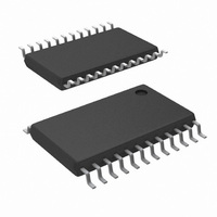
ADC1175-50CIMTX/NOPB National Semiconductor, ADC1175-50CIMTX/NOPB Datasheet - Page 5

ADC1175-50CIMTX/NOPB
Manufacturer Part Number
ADC1175-50CIMTX/NOPB
Description
IC ADC 8BIT 24-TSSOP
Manufacturer
National Semiconductor
Datasheet
1.ADC1175-50CIMTXNOPB.pdf
(20 pages)
Specifications of ADC1175-50CIMTX/NOPB
Number Of Bits
8
Sampling Rate (per Second)
50M
Data Interface
Parallel
Number Of Converters
1
Power Dissipation (max)
125mW
Voltage Supply Source
Analog and Digital
Operating Temperature
-20°C ~ 70°C
Mounting Type
Surface Mount
Package / Case
24-TSSOP (0.173", 4.40mm Width)
Lead Free Status / RoHS Status
Lead free / RoHS Compliant
Other names
*ADC1175-50CIMTX
*ADC1175-50CIMTX/NOPB
ADC1175-50CIMTX
*ADC1175-50CIMTX/NOPB
ADC1175-50CIMTX
Available stocks
Company
Part Number
Manufacturer
Quantity
Price
Company:
Part Number:
ADC1175-50CIMTX/NOPB
Manufacturer:
NS
Quantity:
10 796
DC ACCURACY
INL
DNL
E
E
VIDEO ACCURACY
DP
DG
ANALOG INPUT AND REFERENCE CHARACTERISTIC
V
C
R
BW
R
R
R
I
REF
OT
OB
IN
Symbol
IN
IN
RT
REF
RB
Absolute Maximum Ratings
If Military/Aerospace specified devices are required,
please contact the National Semiconductor Sales Office/
Distributors for availability and specifications.
Converter Electrical Characteristics
The following specifications apply for AV
50% duty cycle. Boldface limits apply for T
Supply Voltage (AV
Voltage on Any Input or Output Pin
Reference Voltage (V
CLK, PD Voltage Range
Digital Output Voltage (V
Input Current at Any Pin (Note 3)
Package Input Current (Note 3)
Power Dissipation at T
ESD Susceptibility (Note 5)
Soldering Temperature, Infrared,
Storage Temperature
Short Circuit Duration
Human Body Model
Machine Model
(10 sec.) (Note 6)
(Single High Output to Ground)
Integral Non Linearity Error
Differential Non-Linearity
Resolution for No Missing
Codes
Top Offset Voltage
Bottom Offset Voltage
Differential Phase Error
Differential Gain Error
Input Range
V
R
Full Power Bandwidth
Top Reference Resistor
Reference Ladder Resistance V
Bottom Reference Resistor
Reference Ladder Current
IN
IN
Input Capacitance
Input Resistance
DD
Parameter
RT
, DV
A
, V
= 25°C
OH
DD
RB
, V
)
)
OL
)
−0.5 to (AV
DD
−65°C to +150°C
V
V
f
f
V
+0.7 Vrms
V
V
= DV
IN
IN
−0.3V to +6.5V
IN
IN
IN
RT
RT
RT
A
= 4.43 MHz Modulated Ramp
= 4.43 MHz Modulated Ramp
= T
= 0.6V to 2.6V
= 0.6V to 2.6V
= 1.5V
See (Note 4)
to V
= V
= V
AV
(Notes 1, 2)
DD
V
DD
MIN
1 Second
SS
SS
RTS
RTS
RB
= +5.0 V
±25 mA
±50 mA
+0.5V)
2000V
to V
to V
235°C
to T
, V
, V
250V
6.5V
RB
RB
DD
DD
MAX
= V
= AV
DC
Conditions
; all other limits T
, PD = 0V, V
RBS
5
SS
Operating Ratings
Package Thermal Resistance
Operating Temperature Range
Supply Voltage (AV
AV
Ground Difference |DV
Pin 11 to Pin 13 Voltage
Upper Reference Voltage (V
Lower Reference Voltage (V
V
V
RT
IN
DD
Voltage Range
- V
(CLK LOW)
(CLK HIGH)
− DV
RT
RB
= +2.6V, V
A
DD
= 25°C (Notes 7, 8).
TSSOP-24
Package
LLP-24
DD
RB
, DV
= 0.6V, C
SS
(Note 9)
Typical
±0.8
+0.7
−0.7
– AV
−12
+10
120
320
270
0.5
1.0
2.0
DD
>1
80
4
7
7
8
RT
RB
)
SS
)
)
(Notes 1, 2)
L
|
= 20 pF, f
(Note 9)
Limits
±1.95
+1.75
−1.0
10.8
12.3
V
92°C / W
40°C / W
V
200
350
5.4
6.1
−20°C
8
RB
RT
θ
+4.75V to +5.25V
JA
CLK
0V to 100 mV
≤
1.0V to V
= 50 MHz at
T
www.national.com
0V to 4.0V
1V to 2.8V
V
A
LSB (max)
LSB (max)
LSB (min)
mA (max)
mA (max)
mA (min)
mA (min)
RB
(Limits)
Ω (max)
V (max)
≤
Ω (min)
V (min)
Units
MHz
Bits
deg
+75°C
MΩ
to V
mV
mV
<0.5V
<0.5V
pF
pF
%
Ω
Ω
DD
RT


