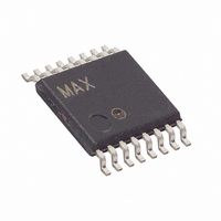
MAX1415EUE+T Maxim Integrated Products, MAX1415EUE+T Datasheet - Page 25

MAX1415EUE+T
Manufacturer Part Number
MAX1415EUE+T
Description
IC ADC 16BIT DELTA SIGMA 16TSSOP
Manufacturer
Maxim Integrated Products
Datasheet
1.MAX1415EUE.pdf
(36 pages)
Specifications of MAX1415EUE+T
Number Of Bits
16
Sampling Rate (per Second)
500
Data Interface
MICROWIRE™, QSPI™, Serial, SPI™
Number Of Converters
1
Power Dissipation (max)
755mW
Voltage Supply Source
Single Supply
Operating Temperature
-45°C ~ 85°C
Mounting Type
Surface Mount
Package / Case
16-TSSOP
Lead Free Status / RoHS Status
Lead free / RoHS Compliant
G2, G1, G0: (Default = 0, 0, 0) Gain-Selection Bits. See
Table 11 for PGA gain settings.
B/U: (Default = 0) Bipolar-/Unipolar-Mode Selection:
Set B/U = 0 to select bipolar mode. Set B/U = 1 to
select unipolar mode.
BUF: (Default = 0) Buffer-Enable Bit. For unbuffered
mode, disable the internal buffer of the MAX1415/
MAX1416 to reduce power consumption by writing a 0 to
the BUF bit. Write a 1 to this bit to enable the buffer. Use
the internal buffer when acquiring high source-imped-
ance input signals.
Table 6. Communications Register
Table 7. Register Selection
*The test register is used for factory testing only.
Table 8. Channel Selection
Table 9. Setup Register
Name
Defaults
Name
Defaults
FUNCTION
FUNCTION
RS2
0
0
0
0
1
1
1
1
CH1
0
0
1
1
RS1
START/DATA READY
(MSB)
0
0
1
1
0
0
1
1
COMMUNICATION
MODE CONTROL
MD1
______________________________________________________________________________________
0
0/DRDY
(MSB)
0
RS0
0
1
0
1
0
1
0
1
MD0
0
CH0
0
1
0
1
G2
RS2
Communications register
0
REGISTER SELECT
PGA GAIN CONTROL
0
Setup register
Offset register
Clock register
Test register*
Data register
No operation
Gain register
REGISTER
16-Bit, Low-Power, 2-Channel,
RS1
0
G1
0
RS0
0
AIN1+
AIN2+
AIN1-
AIN1-
AIN+
G0
0
FSYNC: (Default = 1) Filter-Synchronization/
Conversion-Start Bit. Set FSYNC = 0 to begin calibration
or conversion. The MAX1415/MAX1416 perform free-run-
ning conversions while FSYNC = 0. Set FSYNC = 1 to
stop converting data and to hold the nodes of the digital
filter, the filter-control logic, the calibration-control logic,
and the analog modulator in a reset state. The DRDY
output does not reset high if it is low (indicating that valid
data has not yet been read from the data register) when
FSYNC goes high. To clear DRDY output, read the data
register.
READ/WRITE
BIPOLAR/UNIPOLAR
SELECT
R/W
0
POWER-ON RESET STATUS
MODE
Sigma-Delta ADCs
B/U
0
0x57 61 AB
0x1F 40 00
POWER-DOWN
AIN1-
AIN2-
AIN1-
AIN2-
0x00
0x01
0x85
AIN-
N/A
N/A
—
MODE
PD
0
BUFFER ENABLE
BUF
0
CHANNEL SELECT
REGISTER PAIR
CH1
OFFSET/GAIN
0
REGISTER SIZE
(LSB)
0
1
0
2
(bits)
16
24
24
—
8
8
8
8
FSYNC
FSYNC
CH0
(LSB)
0
1
25


