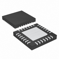
MAX1031BCTI+ Maxim Integrated Products, MAX1031BCTI+ Datasheet - Page 19

MAX1031BCTI+
Manufacturer Part Number
MAX1031BCTI+
Description
IC ADC 10BIT 300KSPS 28-TQFN-EP
Manufacturer
Maxim Integrated Products
Datasheet
1.MAX1027BCEE.pdf
(22 pages)
Specifications of MAX1031BCTI+
Number Of Bits
10
Sampling Rate (per Second)
300k
Data Interface
MICROWIRE™, QSPI™, Serial, SPI™
Number Of Converters
1
Power Dissipation (max)
1.67W
Voltage Supply Source
Single Supply
Operating Temperature
0°C ~ 70°C
Mounting Type
Surface Mount
Package / Case
28-WFQFN Exposed Pad
Lead Free Status / RoHS Status
Lead free / RoHS Compliant
clock. Scanning and averaging are disabled, and the
conversion result is available at DOUT during the con-
version. See Figure 7 for clock mode 11 timing.
Initiate a conversion by writing a byte to the conversion
register followed by 16 SCLK cycles. If CS is pulsed
high between the eighth and ninth cycles, the pulse
width must be less than 100μs. To continuously convert
at 16 cycles per conversion, alternate 1 byte of zeros
between each conversion byte.
If reference mode 00 is requested, or if an external ref-
erence is selected but a temperature measurement is
being requested, wait 65μs with CS high after writing
the conversion byte to extend the acquisition and allow
the internal reference to power up. To perform a tem-
perature measurement, write 24 bytes (192 cycles) of
zeros after the conversion byte. The temperature result
appears on DOUT during the last 2 bytes of the 192
cycles.
If the first byte of an entry in the FIFO is partially read
(CS is pulled high after fewer than 8 SCLK cycles), the
second byte of data that is read out contains the next 8
bits (not b7–b0). The remaining bits are lost for that
entry. If the first byte of an entry in the FIFO is read out
fully, but the second byte is read out partially, the rest
of the entry is lost. The remaining data in the FIFO is
uncorrupted and can be read out normally after taking
CS low again, as long as the 4 leading bits (normally
zeros) are ignored. Internal registers that are written
Figure 7. Clock Mode 11
DIN
SCLK
DOUT
EOC
CS
EXTERNALLY TIMED ACQUISITION, SAMPLING AND CONVERSION WITHOUT CNVST.
Partial Reads and Partial Writes
______________________________________________________________________________________
(ACQUISITION1)
Temp Sensor, Internal Reference
10-Bit 300ksps ADCs with FIFO,
(CONVERSION BYTE)
MSB1
(CONVERSION1)
X = DON'T CARE.
partially through the SPI contain new values, starting at
the MSB up to the point that the partial write is stopped.
The part of the register that is not written contains previ-
ously written values. If CS is pulled low before EOC
goes low, a conversion cannot be completed and the
FIFO is corrupted.
Figure 8 shows the unipolar transfer function for single-
ended or differential inputs. Figure 9 shows the bipolar
transfer function for differential inputs. Code transitions
occur halfway between successive-integer LSB values.
Output coding is binary, with 1 LSB = V
unipolar and bipolar operation, and 1 LSB = 0.125°C
for temperature measurements.
For best performance, use PC boards. Do not use wire-
wrap boards. For the TQFN package, connect its
exposed pad to GND. Board layout should ensure that
digital and analog signal lines are separated from each
other. Do not run analog and digital (especially clock)
signals parallel to one another or run digital lines under-
neath the MAX1027/MAX1029/MAX1031 package. High-
frequency noise in the V
performance. Bypass the V
capacitor to GND, close to the V
itor lead lengths for best supply-noise rejection. If the
power supply is very noisy, connect a 10Ω resistor in
series with the supply to improve power-supply filtering.
Layout, Grounding, and Bypassing
LSB1
(ACQUISITION2)
DD
power supply can affect
DD
DD
Transfer Function
supply with a 0.1μF
pin. Minimize capac-
MSB2
REF
/ 1024V for
19


