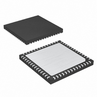
MAX11047ETN+T Maxim Integrated Products, MAX11047ETN+T Datasheet - Page 16

MAX11047ETN+T
Manufacturer Part Number
MAX11047ETN+T
Description
IC ADC 16BIT 250KSPS SAR 56TQFN
Manufacturer
Maxim Integrated Products
Datasheet
1.MAX11047ETN.pdf
(25 pages)
Specifications of MAX11047ETN+T
Number Of Bits
16
Sampling Rate (per Second)
250k
Data Interface
Parallel
Number Of Converters
4
Power Dissipation (max)
2.22W
Voltage Supply Source
Analog and Digital
Operating Temperature
-40°C ~ 85°C
Mounting Type
Surface Mount
Package / Case
56-TQFN Exposed Pad
Lead Free Status / RoHS Status
Lead free / RoHS Compliant
4-/6-/8-Channel, 16-/14-Bit,
Simultaneous-Sampling ADCs
Figure 2. Input Clamp Characteristics
Figures 2 and 3 illustrate the clamp circuit voltage-cur-
rent characteristics for a source impedance R
1280Ω. While the input voltage is within the -300mV to
+(V
clamps. Once the input voltage goes beyond this volt-
age range, the clamps turn on and limit the voltage at
the input pin.
The bidirectional, parallel, digital interface, CR0–CR3,
sets the 4-bit configuration register. This interface
configures the following control signals: chip select
(CS), read (RD), write (WR), end of conversion (EOC),
and convert start (CONVST). Figures 6 and 7 and the
Timing Characteristics in the Electrical Characteristics
table show the operation of the interface.
DB0–DB15/13, output the 16-/14-bit conversion result.
All bits are high impedance when RD = 1 or CS = 1.
CR3 selects the internal or external reference. The POR
default = 0.
0 = internal reference, REFIO internally driven through a
10kΩ resistor, bypass with 0.1µF capacitor to AGND.
1 = external reference, drive REFIO with a high quality
reference.
CR2 selects the output data format. The POR default = 0.
0 = offset binary.
1 = two’s complement.
16
AVDD
______________________________________________________________________________________
+ 300mV) range, no current flows in the input
-10
-15
-20
-25
25
20
15
10
-5
5
0
-30
SIGNAL VOLTAGE AT SOURCE AND CH_ INPUT (V)
R
V
AT SOURCE
AT CH_ INPUT
Applications Information
S
AVDD
= 1170I
-20
= 5.0V
-10
0
CR2 (Output Data Format)
10
CR3 (Int/Ext Reference)
20
Digital Interface
30
40
S
=
Figure 3. Input Clamp Characteristics (Zoom In)
CR1 must be set to 0.
CR0 selects the acquisition mode. The POR default = 0.
0 = CONVST controls the acquisition and conversion.
Drive CONVST low to start acquisition. The rising edge
of CONVST begins the conversion.
1 = acquisition mode starts as soon as previous con-
version is complete. The rising edge of CONVST begins
the conversion.
To program the configuration register, bring the CS and
WR low and apply the required configuration data on
CR3–CR0 of the bus and then raise WR once to save
changes.
CAUTION: The host driving CR3–CR0 must relin-
quish the bus when the conversion results of the
ADC are being read.
CONVST initiates conversions. The devices provide two
acquisition modes set through the configuration regis-
ter. Allow a quiet time (t
conversion to avoid any noise interference during read-
out or write operations from corrupting a sample.
Table 1. Configuration Register
Reference
Int/Ext
CR3
-10
-15
-20
-25
25
20
15
10
-5
5
0
Programming the Configuration Register
-4
SIGNAL VOLTAGE AT SOURCE AND CH_ INPUT (V)
R
V
AT SOURCE
S
AVDD
Data Format
= 1170I
-2
Output
= 5.0V
CR2
0
Q
AT CH_ INPUT
) of 500ns prior to the start of
2
Starting a Conversion
Must be set
4
CR0 (CONVST Mode)
CR1
to 0
6
CR1 (Reserved)
8
CONVST
Mode
CR0


