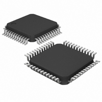
MAX1324ECM+T Maxim Integrated Products, MAX1324ECM+T Datasheet - Page 20

MAX1324ECM+T
Manufacturer Part Number
MAX1324ECM+T
Description
IC ADC 14BIT 8CH 2MSPS 48LQFP
Manufacturer
Maxim Integrated Products
Datasheet
1.MAX1318ECM.pdf
(27 pages)
Specifications of MAX1324ECM+T
Number Of Bits
14
Sampling Rate (per Second)
2M
Data Interface
Parallel
Number Of Converters
1
Power Dissipation (max)
1.82W
Voltage Supply Source
Analog and Digital
Operating Temperature
-40°C ~ 85°C
Mounting Type
Surface Mount
Package / Case
48-LQFP
Lead Free Status / RoHS Status
Lead free / RoHS Compliant
8-/4-/2-Channel, 14-Bit, Simultaneous-Sampling ADCs
with ±10V, ±5V, and 0 to +5V Analog Input Ranges
No other digital system ground should be connected to
this single-point analog ground. The ground return to
the power supply for this ground should be low imped-
ance and as short as possible for noise-free operation.
High-frequency noise in the V
affect the high-speed comparator in the ADC. Bypass
these supplies to the single-point analog ground with
0.1µF and 2.2µF bypass capacitors close to the device.
If the +5V power supply is very noisy, a ferrite bead can
be connected as a lowpass filter, as shown in Figure 8.
Table 5 and Figure 9 show the two’s complement trans-
fer function for the MAX1324/MAX1325/MAX1326 with a
±10V input range. The full-scale input range (FSR) is
eight times the voltage at REF. The internal +2.500V ref-
erence gives a +20V FSR, while an external +2V to +3V
reference allows an FSR of +16V to +24V, respectively.
Calculate the LSB size using the following equation:
This equals 1.2207mV with a +2.5V internal reference.
Table 5. ±10V Bipolar Code Table
20
BINARY OUTPUT CODE
TWO’S COMPLEMENT
01 1111 1111 1111
01 1111 1111 1110
00 0000 0000 0001
00 0000 0000 0000
11 1111 1111 1111
10 0000 0000 0001
10 0000 0000 0000
______________________________________________________________________________________
0x1FFE
0x1FFF
0x0001
0x0000
0x3FFF
0x2001
0x2000
LSB
=
EQUIVALENT
8
DECIMAL
(CODE
OUTPUT
×
2
-8191
-8192
Transfer Functions
8191
8190
14
DD
V
-1
1
0
Bipolar ±10V Devices
REF
10
power supply may
)
VOLTAGE (V)
(V
V
REF
±0.5 LSB
±0.5 LSB
±0.5 LSB
±0.5 LSB
±0.5 LSB
±0.5 LSB
±0.5 LSB
MSV
-0.0006
-9.9982
-9.9994
9.9994
9.9982
0.0018
0.0006
INPUT
= 2.5V,
= 0V)
The input range is centered about V
MSV = AGND, and the input is symmetrical about zero.
For a custom midscale voltage, drive MSV with an
external voltage source. Noise present on MSV directly
couples into the ADC result. Use a precision, low-drift
voltage reference with adequate bypassing to prevent
MSV from degrading ADC performance. For maximum
FSR, be careful not to violate the absolute maximum
voltage ratings of the analog inputs when choosing
V
Determine the input voltage as a function of V
V
ing equation:
Table 6 and Figure 10 show the two’s complement
transfer function for the MAX1320/MAX1321/MAX1322
with a ±5V input range. The FSR is four times the volt-
age at REF. The internal +2.500V reference gives a
+10V FSR, while an external +2V to +3V reference
allows an FSR of +8V to +12V, respectively. Calculate
the LSB size using the following equation:
This equals 0.6104mV when using the internal reference.
Figure 9. ±10V Bipolar Transfer Function
MSV
MSV
0x1FFD
0x1FFC
.
, and the output code in decimal using the follow-
0x1FFF
0x1FFE
0x0001
0x0000
0x3FFF
0x2003
0x2002
0x2001
0x2000
V
CH
-8192 -8190
_
=
LSB
LSB
INPUT VOLTAGE (V
=
×
CODE
4
-1 0 +1
8 x V
×
(MSV)
2
CH_
14
REF
V
10
REF
- V
Bipolar ±5V Devices
MSV
+
1 LSB =
IN LSBs)
V
MSV
MSV
+8189
8 x V
. Normally,
2
14
+8191
REF
8 x V
REF
REF
,


