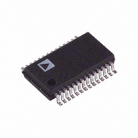
AD9224ARS Analog Devices Inc, AD9224ARS Datasheet

AD9224ARS
Specifications of AD9224ARS
Available stocks
Related parts for AD9224ARS
AD9224ARS Summary of contents
Page 1
FEATURES Monolithic 12-Bit, 40 MSPS A/D Converter Low Power Dissipation: 415 mW Single +5 V Supply No Missing Codes Guaranteed Differential Nonlinearity Error: Complete On-Chip Sample-and-Hold Amplifier and Voltage Reference Signal-to-Noise and Distortion Ratio: 68.3 dB Spurious-Free Dynamic Range: ...
Page 2
AD9224–SPECIFICATIONS DC SPECIFICATIONS (AVDD = +5 V, DRVDD = + Parameter RESOLUTION MAX CONVERSION RATE INPUT REFERRED NOISE VREF = 1.0 V VREF = 2.0 V ACCURACY Integral Nonlinearity (INL) Differential Nonlinearity (DNL) No Missing Codes Guaranteed Zero ...
Page 3
AC SPECIFICATIONS (AVDD = +5 V, DRVDD = + Parameter SIGNAL-TO-NOISE AND DISTORTION RATIO (S/N+ 2.5 MHz INPUT MHz INPUT SIGNAL-TO-NOISE RATIO (SNR 2.5 MHz INPUT MHz INPUT ...
Page 4
... CLOCK DATA OUTPUT Figure 1. Timing Diagram Model Temperature Range AD9224ARS – +85 C AD9224-EB CAUTION ESD (electrostatic discharge) sensitive device. Electrostatic charges as high as 4000 V readily accumulate on the human body and test equipment and can discharge without detection. Although the AD9224 features proprietary ESD protection circuitry, permanent damage may occur on devices subjected to high energy electrostatic discharges ...
Page 5
DEFINITIONS OF SPECIFICATION INTEGRAL NONLINEARITY (INL) INL refers to the deviation of each individual code from a line drawn from “negative full scale” through “positive full scale.” The point used as “negative full scale” occurs 1/2 LSB before the first ...
Page 6
AD9224 Typical Performance Characteristics 1.00 0.75 0.50 0.25 0.00 –0.25 –0.50 –0.75 –1.00 0 511 1022 1533 2044 2555 CODE Title Figure 2. Typical DNL 75 70 –0.5dB 65 –6.0dB 60 55 –20.0dB 0 ...
Page 7
SFDR SNR –0.5 –20 INPUT AMPLITUDE Figure 8. SNR/SFDR vs. A (Input Amplitude Input Span = 4 2.5 V Differential Input SNR ...
Page 8
AD9224 INTRODUCTION The AD9224 is a high performance, complete single-supply 12- bit ADC. The analog input range of the AD9224 is highly flex- ible allowing for both single-ended or differential inputs of varying amplitudes that can ...
Page 9
Due to the high degree of symmetry within the SHA topology, a significant improvement in distortion performance for differ- ential input signals with frequencies up to and beyond Nyquist can be realized. This inherent symmetry provides excellent cancellation of both ...
Page 10
AD9224 REFERENCE OPERATION The AD9224 contains an onboard bandgap reference that provides a pin strappable option to generate either output. With the addition of two external resistors, the user can generate reference voltages other ...
Page 11
Input Input Connection Coupling Span (V) Single-Ended VREF 4 2 VREF Single-Ended VREF 4 2 VREF Differential AC/DC 2 (via Transformer) or Amplifier 2 VREF 4.0 NOTE 1 VINA and VINB can be ...
Page 12
AD9224 DRIVING THE ANALOG INPUTS The AD9224 has a highly flexible input structure allowing it to interface with single-ended or differential input interface cir- cuitry. The applications shown in Driving the Analog Inputs and Reference Configurations sections, along with the ...
Page 13
Simple Op Amp Buffer In the simplest case, the input signal to the AD9224 will already be biased at levels in accordance with the selected input range simply necessary to provide an adequately low source imped- ance for ...
Page 14
AD9224 Alternative AC Interface Figure 22 shows a flexible ac-coupled circuit that can be con- figured for different input spans. Since the common-mode voltage of VINA and VINB are biased to midsupply (V independent of VREF, VREF can be pin ...
Page 15
The driver circuit shown in Figure 23 is optimized for dc cou- pling applications requiring optimum distortion performance. This differential op amp driver circuit is configured to convert and level shift p-p single-ended, ground referenced signal to ...
Page 16
AD9224 REFERENCE CONFIGURATIONS The figures associated with this section on internal and external reference operation do not show recommended matching series resistors for VINA and VINB for the purpose of simplicity. Please refer to the Driving the Analog Inputs section ...
Page 17
Resistor Programmable Reference Figure 28 shows an example of how to generate a reference voltage other than 1 2.0 V with the addition of two exter- nal resistors and a bypass capacitor. Use the equation, VREF = 1 ...
Page 18
AD9224 DIGITAL INPUTS AND OUTPUTS Digital Outputs The AD9224 output data is presented in positive true straight binary for all input ranges. Table IV indicates the output data formats for various input ranges regardless of the selected input range. A ...
Page 19
In this case an 80 MHz clock is divided by two to produce the 40 MHz clock input for the AD9224. In this configuration, the duty cycle of the 80 MHz clock is irrelevant. The input circuitry for the CLOCK ...
Page 20
AD9224 The distortion and noise performance of an ADC at the given IF frequency is of particular concern when evaluating an ADC for a narrowband IF sampling application. Both single tone and dual tone SFDR vs. amplitude are very useful ...
Page 21
GROUNDING AND DECOUPLING Analog and Digital Grounding Proper grounding is essential in any high speed, high resolution system. Multilayer printed circuit boards (PCBs) are recom- mended to provide optimal grounding and power schemes. The use of ground and power planes ...
Page 22
AD9224 U5 REF43 6 2 VOUT VIN 1 GND 1 C18 C30 + 0.1 F R31 2 10V R25 2 820 2.49k 2 2 JP19 C29 ...
Page 23
Figure 45. Evaluation Board Component Side Layout (Not to Scale) Figure 46. Evaluation Board Ground Plane Layout (Not to Scale) Figure 47. Evaluation Board Component Side Silkscreen (Not to Scale) REV. A Figure 48. Evaluation Board Solder Side Layout (Not ...
Page 24
AD9224 0.078 (1.98) 0.068 (1.73) 0.008 (0.203) 0.002 (0.050) OUTLINE DIMENSIONS Dimensions shown in inches and (mm). 28-Lead Shrink Small Outline (SSOP) (RS-28) 0.407 (10.34) 0.397 (10.08 0.07 (1.79) PIN 1 0.066 (1.67) 8° 0.0256 0.015 ...


