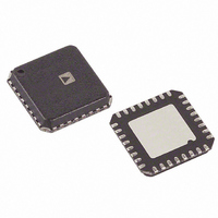
AD7490BCP-REEL7 Analog Devices Inc, AD7490BCP-REEL7 Datasheet - Page 17

AD7490BCP-REEL7
Manufacturer Part Number
AD7490BCP-REEL7
Description
IC ADC 12BIT 16CH 32-LFCSP T/R
Manufacturer
Analog Devices Inc
Datasheet
1.AD7490BRUZ.pdf
(28 pages)
Specifications of AD7490BCP-REEL7
Rohs Status
RoHS non-compliant
Number Of Bits
12
Sampling Rate (per Second)
1M
Data Interface
DSP, MICROWIRE™, QSPI™, Serial, SPI™
Number Of Converters
1
Power Dissipation (max)
12.5mW
Voltage Supply Source
Single Supply
Operating Temperature
-40°C ~ 85°C
Mounting Type
Surface Mount
Package / Case
32-VFQFN, CSP Exposed Pad
For Use With
EVAL-AD7490CBZ - BOARD EVAL CONTROL FOR AD7490
When no amplifier is used to drive the analog input, the source
impedance should be limited to low values. The maximum
source impedance depends on the amount of total harmonic
distortion (THD) that can be tolerated. The THD increases as
the source impedance increases, and performance degrades (see
Figure 9).
ADC TRANSFER FUNCTION
The output coding of the AD7490 is either straight binary or
twos complement depending on the status of the LSB
(CODING bit) in the control register. The designed code
transitions occur midway between successive LSB values (that
is, 1 LSB, 2 LSBs, and so on). The LSB size is equal to
REF
when straight binary coding is selected is shown in Figure 18.
IN
/4096. The ideal transfer characteristic for the AD7490
0V
V
V
000...010
000...001
000...000
111...000
111...110
011...111
111...111
REF
Figure 18. Straight Binary Transfer Characteristic
IS EITHER REF
0V
V
REF
1LSB
0.1µF
IN
OR 2 × REF
V
ANALOG INPUT
R1 = R2 = R3 = R4
R3
R2
IN
1LSB = V
+V
R4
R1
REF
REF
/4096
– 1LSB
REF
V
V
IN
IN
Figure 20. Handling Bipolar Signals
0
15
AD7490
IN
V
DD
V
Rev. C | Page 17 of 28
DOUT
DRIVE
COMPLEMENT
TWOS
Handling Bipolar Input Signals
Figure 20 shows how useful the combination of the 2 × REF
input range and the twos complement output coding scheme is
for handling bipolar input signals. If the bipolar input signal is
biased about REF
selected, REF
full scale, and +REF
dynamic range of 2 × REF
DSP/µP
000...001
000...000
100...010
100...001
100...000
011...111
011...110
111...111
Figure 19. Twos Complement Transfer Characteristic
IN
becomes the zero code point, −REF
V
–V
DD
IN
REF
with REF
and twos complement output coding is
IN
(= 2 × REF
+ 1LSB
becomes positive full scale, with a
+REF
–REF
REF
(= 0V)
IN
IN
V
.
IN
± REF
REF
IN
IN
IN
ANALOG INPUT
)
– 1LSB
1LSB = 2 × V
IN
Input Range
+V
REF
– 1LSB
REF
/4096
011...111
000...000
100...000
IN
AD7490
is negative
IN


