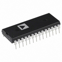
AD7862AN-3 Analog Devices Inc, AD7862AN-3 Datasheet - Page 4

AD7862AN-3
Manufacturer Part Number
AD7862AN-3
Description
IC ADC 12BIT DUAL 250KSPS 28-DIP
Manufacturer
Analog Devices Inc
Datasheet
1.AD7862ARZ-10.pdf
(16 pages)
Specifications of AD7862AN-3
Rohs Status
RoHS non-compliant
Number Of Bits
12
Sampling Rate (per Second)
250k
Data Interface
Parallel
Number Of Converters
2
Power Dissipation (max)
75mW
Voltage Supply Source
Analog and Digital
Operating Temperature
-40°C ~ 85°C
Mounting Type
Through Hole
Package / Case
28-DIP (0.600", 15.24mm)
AD7862
TIMING CHARACTERISTICS
Parameter
t
t
Parallel Interface
t
t
t
t
t
t
t
NOTES
1
2
3
4
Specifications subject to change without notice.
CAUTION
ESD (electrostatic discharge) sensitive device. Electrostatic charges as high as 4000 V readily
accumulate on the human body and test equipment and can discharge without detection.
Although the AD7862 features proprietary ESD protection circuitry, permanent damage may
occur on devices subjected to high energy electrostatic discharges. Therefore, proper ESD
precautions are recommended to avoid performance degradation or loss of functionality.
Sample tested at +25 C to ensure compliance. All input signals are measured with tr = tf = 1 ns (10% to 90% of +5 V) and timed from a voltage level of +1.6 V.
Measured with the load circuit of Figure 2 and defined as the time required for an output to cross 0.8 V or 2.0 V.
These times are derived from the measured time taken by the data outputs to change 0.5 V when loaded with the circuit of Figure 2. The measured number is then
CONV
ACQ
1
2
3
4
5
6
7
extrapolated back to remove the effects of charging or discharging the 50 pF capacitor. This means that the times quoted in the timing characteristics are the true bus
relinquish times of the part and as such are independent of external bus loading capacitances.
See Figure 1.
3
4
CONVST
BUSY
DATA
A, B
Versions
3.6
0.3
0
0
35
35
12
60
5
30
40
RD
CS
A0
Figure 2. Load Circuit for Access Time and Bus Relinquish Time
t
3
t
1, 2
CONV
(V
otherwise noted.)
t
5
DD
S
Version
3.6
0.3
0
0
45
45
12
70
5
40
40
t
OUTPUT
1
= +5 V
V
Figure 1. Timing Diagram
t
4
PIN
A1
TO
.........
50pF
5%, AGND = DGND = 0 V, REF = Internal. All Specifications T
t
6
V
A2
–4–
t
2
Units
us max
ns min
ns min
ns min
ns min
ns min
ns max
ns min
ns max
ns min
s max
1.6mA
200µA
+1.6V
V
Test Conditions/Comments
Conversion Time
Acquisition Time
CS to RD Setup Time
CS to RD Hold Time
CONVST Pulse Width
Read Pulse Width
Data Access Time After Falling Edge of RD
Bus Relinquish Time After Rising Edge of RD
Time Between Consecutive Reads
B1
.........
t
7
V
B2
WARNING!
ESD SENSITIVE DEVICE
MIN
to T
MAX
REV. 0
unless


