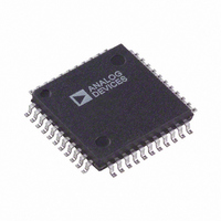
AD9054ABST-135 Analog Devices Inc, AD9054ABST-135 Datasheet - Page 15

AD9054ABST-135
Manufacturer Part Number
AD9054ABST-135
Description
IC ADC 8BIT 135MSPS 44-LQFP
Manufacturer
Analog Devices Inc
Datasheet
1.AD9054ABSTZ-135.pdf
(20 pages)
Specifications of AD9054ABST-135
Rohs Status
RoHS non-compliant
Number Of Bits
8
Sampling Rate (per Second)
135M
Data Interface
Parallel
Number Of Converters
1
Power Dissipation (max)
700mW
Voltage Supply Source
Single Supply
Operating Temperature
-40°C ~ 85°C
Mounting Type
Surface Mount
Package / Case
44-LQFP
Available stocks
Company
Part Number
Manufacturer
Quantity
Price
Company:
Part Number:
AD9054ABST-135
Manufacturer:
FUJI
Quantity:
149
Company:
Part Number:
AD9054ABST-135
Manufacturer:
ADI
Quantity:
225
Part Number:
AD9054ABST-135
Manufacturer:
ADI/亚德诺
Quantity:
20 000
EVALUATION BOARD
The AD9054A evaluation board offers an easy way to test the
AD9054A. It provides dc biasing for the analog input, generates
the latch clocks for both full speed and demuxed modes, and
includes a reconstruction DAC. The board has several different
modes of operation, and is shipped in the following configuration:
• DC-Coupled Analog Input
• Demuxed Outputs
• Differential Clocks
• Internal Voltage Reference.
Analog Input
The evaluation board accepts a 1 V input signal centered at
ground. The board’s input circuitry then biases this signal to
2.5 V in one of two ways:
1. DC-coupled through an AD9631 op amp; this is the mode in
2. AC-coupled through C1.
These two modes are selected by jumpers S101 and S103. For
dc coupling, the S101 jumper is connected between the two left
pins and the S103 jumper is connected between the two lower
pins. For ac coupling, the S101 jumper is connected between
the two right pins and the S103 jumper is connected between
the two upper pins.
ENCODE
The AD9054A ENCODE input can be driven two ways:
1. Differential TTL, CMOS, or PECL; it is shipped in this
2. Single-ended TTL or CMOS. To use in this mode, remove
AIN
S105
which it is shipped. Potentiometer R7 provides adjustment of
the bias voltage.
mode.
R11, the 50 Ω chip resistor located next to the ENCODE
input, and insert a 0.1 µF ceramic capacitor into the C5 slot.
C5 is located between the ENC connector and the ENCODE
input to the DUT and is marked on the back side of the
board. In this mode, ENCODE is biased with internal resis-
tors to 1.5 V, but it can be externally driven to any dc voltage.
50
ENC
ENC
RESET
BUTTON
C
D
CLK A
CLK B
D FF
50
50
DC BIAS
5V
S103
S102
S104
ENC
ENC
VREF EXT
VREF OUT
VREF IN
AIN
AIN
DEMUX
DS DS ENC ENC
CLOCKING
AD9054A
CLK A
CLK B
B PORT
A PORT
DAC
'574
'574
Voltage Reference
The AD9054A has an internal 2.5 V voltage reference. An
external reference may be employed instead. The evaluation
board is configured for the internal reference. To use an external
reference, connect it to the (VREF) pin on the power connector
and move jumper S102.
Single Port Mode
Single Port Mode sets the AD9054A to produce data on every
clock cycle on output port A only. To test in this mode, jumper
S104 should be set to single channel and S106 and S107 must
be set to F (for Full). The maximum speed in single port mode
is 100 MSPS.
Dual Port Mode
Dual Port or half-speed output mode sets the ADC to produce
data alternately on Port A and Port B. In this mode, the reset
function should be implemented. To test in this mode, set
jumper S104 to Dual Channel, and set S106 and S107 to D (for
Dual Port). The maximum speed in this mode is 200 MSPS.
RESET
RESET drives the AD9054A’s Data Sync (DS) pins. When
operating in Single Port Mode, RESET is not used. In Dual-
Channel Mode it is needed for two reasons: to synchronize the
timing of Port A data and Port B data with a known clock edge,
as described in the data sheet, and to synchronize the evaluation
board’s latch clocks with the data coming out of the AD9054A.
Reset can be driven in two ways: by pushing the reset button on
the board, or externally, with a TTL pulse through connector
J5 or J6.
DAC Out
The DAC output is a representation of the data on output Port
A only. Output Port B is not reconstructed.
Troubleshooting
If the board does not seem to be working correctly, try the
following:
• Check that all jumpers are in the correct position for the
• Push the reset button. This will align the AD9054A’s data
• Switch the jumper S105 from A-R to R-B or vice-versa, then
• At high encode rates, the evaluation board’s clock generation
The AD9054A Evaluation Board is provided as a design example
for customers of Analog Devices, Inc. ADI makes no warranties,
express, statutory, or implied, regarding merchantability or
fitness for a particular purpose.
desired mode of operation.
output with the half speed latch clocks.
push the reset button. In demuxed mode, this will have the
effect of inverting the half speed latch clocks.
circuitry is sensitive to the 5 V digital power supply. At high
encode rates, the 5 V digital power should be kept below
5.2 V. This is an evaluation board sensitivity and not an
AD9054A sensitivity.
AD9054A


