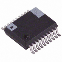
AD9057BRS-RL60 Analog Devices Inc, AD9057BRS-RL60 Datasheet - Page 4

AD9057BRS-RL60
Manufacturer Part Number
AD9057BRS-RL60
Description
IC ADC 8BIT 60MSPS 20-SSOP T/R
Manufacturer
Analog Devices Inc
Datasheet
1.AD9057BRSZ-RL40.pdf
(12 pages)
Specifications of AD9057BRS-RL60
Rohs Status
RoHS non-compliant
Number Of Bits
8
Sampling Rate (per Second)
60M
Data Interface
Parallel
Number Of Converters
1
Power Dissipation (max)
260mW
Voltage Supply Source
Analog and Digital
Operating Temperature
-40°C ~ 85°C
Mounting Type
Surface Mount
Package / Case
20-SSOP (0.200", 5.30mm Width)
Available stocks
Company
Part Number
Manufacturer
Quantity
Price
Company:
Part Number:
AD9057BRS-RL60
Manufacturer:
Panasonic
Quantity:
1 310
Part Number:
AD9057BRS-RL60
Manufacturer:
ADI/亚德诺
Quantity:
20 000
ABSOLUTE MAXIMUM RATINGS*
V
Analog Inputs . . . . . . . . . . . . . . . . . . . . –0.5 V to V
Digital Inputs . . . . . . . . . . . . . . . . . . . –0.5 V to V
VREF Input . . . . . . . . . . . . . . . . . . . . . . –0.5 V to V
Digital Output Current . . . . . . . . . . . . . . . . . . . . . . . . 20 mA
Operating Temperature . . . . . . . . . . . . . . . . –55∞C to +125∞C
Storage Temperature . . . . . . . . . . . . . . . . . . –65∞C to +150∞C
Maximum Junction Temperature . . . . . . . . . . . . . . . . 150∞C
Maximum Case Temperature . . . . . . . . . . . . . . . . . . . 150∞C
*Stresses above those listed under Absolute Maximum Ratings may cause perma-
Model
AD9057BRS-40
AD9057BRS-60
AD9057BRS-80
AD9057/PCB
*RS = Shrink Small Outline Package (SSOP).
Analog Input
3.0 V
2.502 V
2.498 V
2.0 V
AD9057
CAUTION
ESD (electrostatic discharge) sensitive device. Electrostatic charges as high as 4000 V readily
accumulate on the human body and test equipment and can discharge without detection. Although
the AD9057 features proprietary ESD protection circuitry, permanent damage may occur on
devices subjected to high energy electrostatic discharges. Therefore, proper ESD precautions are
recommended to avoid performance degradation or loss of functionality.
nent damage to the device. This is a stress rating only; functional operation of the
device at these or any other conditions above those listed in the operational
sections of this specification is not implied. Exposure to absolute maximum rating
conditions for extended periods may affect device reliability.
D
, V
DD
. . . . . . . . . . . . . . . . . . . . . . . . . . . . . . . . . . . . . . . 7 V
Table I. Digital Coding (VREF = 2.5 V)
Voltage Level
Positive Full Scale
Midscale +1/2 LSB
Midscale –1/2 LSB
Negative Full Scale
ORDERING GUIDE
Temperature
Range
–40∞C to +85∞C RS-20
–40∞C to +85∞C RS-20
–40∞C to +85∞C RS-20
25∞C
Package Option*
Evaluation Board
Digital Output
1111 1111
1000 0000
0111 1111
0000 0000
DD
D
D
+ 0.5 V
+ 0.5 V
+ 0.5 V
–4–
Pin No.
1
2
3
4, 9, 16
5, 8
6
7
10
11–14, 17–20
15
PIN FUNCTION DESCRIPTIONS
Mnemonic
PWRDN
VREF OUT
VREF IN
GND
V
BIAS OUT
AIN
ENCODE
D7–D0
V
VREF OUT
BIAS OUT
ENCODE
D
DD
VREF IN
PWRDN
PIN CONFIGURATION
GND
GND
AIN
V
V
D
D
10
1
2
3
4
5
6
7
8
9
(Not to Scale)
TOP VIEW
AD9057
Function
Power-Down Function Select;
Logic High for Power-Down
Mode (Digital Outputs Go to
High Impedance State).
Internal Reference Output
(2.5 V typ); Bypass with 0.1 mF
to Ground.
Reference Input for ADC (2.5 V
typ, ± 10%).
Ground (Analog/Digital).
Analog 5 V Power Supply.
Bias Pin for AC Coupling
(1 kW to REF IN).
Analog Input for ADC.
Encode Clock for ADC (ADC
Samples on Rising Edge of
Encode).
Digital Outputs of ADC.
Digital Output Power Supply;
Nominally 3 V to 5
WARNING!
20
19
18
17
16
15
14
13
12
11
D0 (LSB)
D1
D2
D3
GND
V
D4
D5
D6
D7 (MSB)
DD
ESD SENSITIVE DEVICE
V.
REV. D


